This thread has been locked.

If you have a related question, please click the "Ask a related question" button in the top right corner. The newly created question will be automatically linked to this question.

TPS63700: TPS63700: IC failing very often

Part Number: TPS63700


Tool/software:

Hello

I have implemented this DCDC to generate a -5.4V output. The source is a very stable 3.3V output from a DCDC (with 3A max output) .
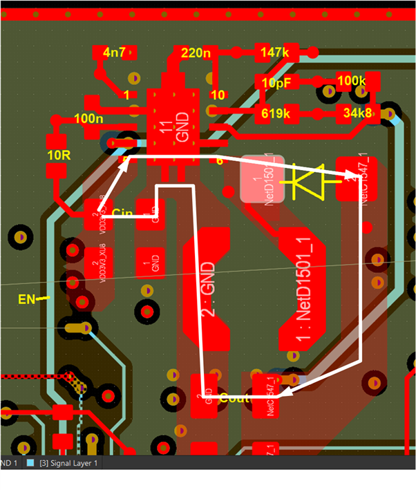
I really copied the design from the datasheet more or less. No magic here.
The output load is 30mA only! The load is an LDO to generate -5V for an analog circuit.

The EN signal comes 14ms after the 3.3V is stable.

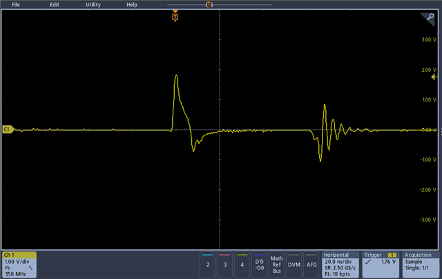
I have now 21 boards of which 8 boards have a failure on this DCDC.

They all show a very similar behaviour:
I see +0.65V on the output. The 10R VIN resistor has a drop of about 1.5V, leaving about 1.7V at the VIN. So the current going into VIN is about 150mA. 
So I assume this IC is dead. 
Could be anything else than ESD be the reason? Can pre-bias kill this IC? We are using sometimes this board with no load attached for R&D reasons.

The COMP cap C107 and 220nF from VREF C102 are totally at the PCB edge. So when you hold the PCB with your fingers on the edge, you will touch those caps. 
We do have ESD shoes etc, but not an ESD floor. 

Is it known that this IC is so super sensible?

Thanks for any inputs! I really don't know what else it could be, but almost 50% failure is too high to just say "it's ESD" it seems.

  • Hi Michel,

    Please share layout of this IC and part number of Cout.

    Also, please use multimeter diode mode and measure the diode between VIN and SW, check the diode voltage for both VIN to SW and from SW to VIN.

    Best Regards,

    Travis


  • Here is the layout of the TOP (red), L1 (GND plane in olive-green) and the feedback trace on L3 (light blue)

    I measured also as you wrote 2 broken boards and one good board with the diode tester. Results were all the same:

    Diode (SW) + / Cin (IN) -: 0.354 - 0.356V
    Diode (SW) - / Cin (IN) + : 0.946 - 0.964V

    Cout is a generic 47uF MLCC with 10V X5R 0805 20% specs. The assembly factory put what they had on hand. But I am sure from a known brand, no cheap stuff, it's an Austrian factory with good reputation. 

  • Hi Michel,

    For inverting buck-boost topology, high frequency switching current goes from Vin->SW->Vout->Vin. Parasitic inductance within this current loop will arouse switching ringing and the MOSFET will damage if the switching spike goes over the MOSFET BVDSS. So it's very important to reduce the PCB length of this current loop. For EVM, this current loop goes like this:

    while your layout:

    So I recommend adding a 100nf here and fill the polygon in the white block

    Best Regards,

    Travis

  • Hello Travis

    Thanks for the inputs. I will add your propositions for the next layout change!

    I added the 100nF on my exisiting design and it really reduced the ringing spike. Here the AC view of the output voltage after the inductor without the 100nF:


    Then with the 100nF cap with same 1V/div:


    But as I decribed above, it seems that the logic part is broken. The inside FET seems to have measure the same on a good or bad board, so I guess the FET is fine? Could this destroy the internal logic part??
    I do measure spikes on the VIN pin of about 200mVpp without the 100nF and about 100mVpp with the 100nF. Nothing that I would expect the DCDC VIN logic input to die on me?

    Beware, here I loaded the DCDC with a 108mA resistive load. I only have about 30mA load in my application.

  • Hi Michel,

    It's not normal that the diode can be measured from VIN+ to SW-. Can you confirm again with the IC removed from the board? 

    It's very hard to tell what impact there'll be within the IC, so I think you can apply the 100nf and try again. The fail rate is 8/20 so I assume it should be very easy to repeat the damage if the probmen is not fixed.

    Best Regards,

    Travis

  • Ah, I had other loads on the 3.3V input that were measured over the inductor back to GND.

     I removed the inductor and now I measure on a bad board 0.439V with IN - and SW +. The other way around no flow, so the FET is good as I expected.

    It's really the logic part. I could see a difference when I measure the VIN to GND. 
    I removed the 10R to be able to measure on a good board with VIN + and GND - nothing (OL) with the diode meter. With a bad board I did the same, but I can measure 1.47V. Also on the COMP and VREF inputs I see a difference with the diode meter compared to a good board. So I really think as I wrote above the logic part is damaged of all those boards.

    The 200Vpp spikes on the input don't really explain why this IC's die, does it?

    But yeah, I will add the 100nF on the boards, that's for sure!

  • Hi Michel,

    The switching spike couples to everywhere and it's very hard to tell which part of the circuit would kill first. I didn't see and other incorrect design in your schematic or layout so I recommend optimizing layout and see if the problem still occurs.

    Best Regards,

    Travis

  • Ok, thank you! I will then modify all with this 100nF and see if we still have those failures in future! They usually don't die very fast, it took a few weeks on some, on others even longer to die on us.