Other Parts Discussed in Thread: LM5122, LM5125-Q1, TPA3223, LM5126-Q1
Tool/software:
Hi all,
i would have to questions about the Usage of the LM5123.
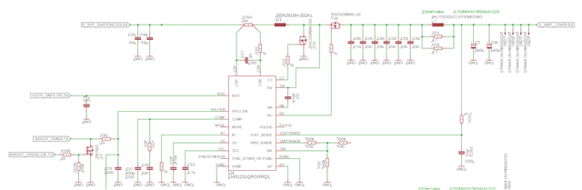
1. BIAS Supply: Is it possible to use a separate Buck Converter (V_IN to 6V) to supply this Pin instead of V_IN or V_OUT? The losses from the internal LDO generating the 5V VDD could be minimized like that. According to the datasheet, this is OK, but in all application diagrams, Schematics, Eval etc. it is never done.
2. Usage of a Output LC Filter: According to the Datasheet, the V_SENSE Pin must be connected to the Drain of the Highside FET. Usually, i would include an LC Output Filter in the Sensing Loop to a) avoid stabiltiy issues, b) improve voltage accuracy.
The actual application has a number of ceramic capacitors on the Output, followed by a Inductor, more ceramics and the bulk elkos. Like this, the Current Load on the Electrolytics is lowered a lot, but the ripple on the drain of the mosfet is quite high. With "classical" boost Converters as the LM5122, i usually conenct the sensing pin at the bulk elcos without an issue, but i'm, unsure how to implement this with the LM5123.
thanks a lot for tips and tricks here!
Best regards,
Lukas