This thread has been locked.

If you have a related question, please click the "Ask a related question" button in the top right corner. The newly created question will be automatically linked to this question.

LMG2100R026: What compact options for high duty cycle commuting ?

Part Number: LMG2100R026

Tool/software:

Tool/software:

Hi,

I'm designing a compact FOC controller with LMG2100R026

Board space is at a premium.
I would also like to maximize acceptable voltage at the motor, which means having, at time, high duty cycle.

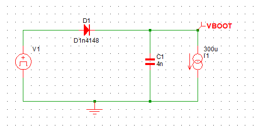
My understanding is that, for "normal conditions", the maximum duty cycle is roughly 67% (100nF bootstrap capacitor, 100mA charging current, 100kHZ operating frequency, 8mA operating current)

I'm looking for ways to keep the bootstrap capacitor topped up.


I understand there are 3 possibilities:
- Use of a low capacitance isolated DCDC.
An affordable option is R05C1TF05S-R or MIE1W0505BGLVH, but it is somewhat bulky
I could also use an ILDC12, but they are a bit pricey (like, same price as LMG2100R026 or so), and don't have great voltage regulation (4.5->5.5V)

- Use of a charge pump.
This has several limits. Besides polluting my 5V rail with each swing of the output (thanks to the high V/ns of LMG2100), it has quite low efficiency when VBUS = 90V

- Use of a boost circuit.
This would be my preferred solution. No capacitive coupling with my 5V rail, modularity, compactness etc.

Here are 3 options, based on values I calculated.


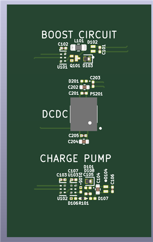
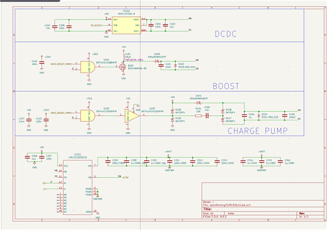
Note : while and-gates are not necessary, they prevent wasting energy pumping into a low bridge.

Is there a reason _not_ to use the boost circuit ?

Thanks

  • Hi Elie, 

    If the maximum high-side duty cycle is 67%, it shouldn't be too challenging to use a typical bootstrap circuit for the high-side. The challenge for bootstrap circuits arise when the duty cycle approaches higher than ~90% or so. 

    The main issue with the boost circuit is the fact that it is not regulated. This becomes challenging as the load of the boost converter is the current consumed by the VCC pin which is load dependent. This variation in load would potentially cause the boost converter to alternate between CCM and DCM, changing the output voltage significantly. 

    Have you simulated the worst-case condition using a typical bootstrap circuit? If you prefer using another solution other than bootstrap for high duty cycles, I would recommend the isolated bias supply. 

    Thanks,

    John 

  • Thanks for your answer.

    I could argue that you could somewhat regulate the output with the boost circuit, thanks to the zener and thanks to the opportunity to modulate the PWM.

    I have not simulated the LMG2100. I have more of a firmware background, so I'm not too familiar with the simulation suites available with this device. Do you have a suggestion ? I read that PLECS and Simplis models are available.

    But I will follow your advice, bite the bullet and add 3xN DC DC isolated supply to my BOM

    Thanks

    Elie

  • You could use the released SIMPLIS model that is available. 

    However, I was just referring to a simple simulation to analyze the requirements needed for a simple bootstrap circuit. In this simulation, you would have a switching function, a diode, a capacitor, and  a load, as shown below:

    The switching function would be set according to your lowest switching frequency and duty cycle for the low-side FET, and the load would be set to the HB pin consumption of LMG2100. 

    Thanks,

    John

  • Ah, this kind of simulation.

    I did a "tabletop" simulation, but most likely wrongly. It's how I arrived to the 67%.

    Let me go back to my calculations.

    In the time being, thanks again for your help. Let me validate your answer

    Elie

  • By the way, the image above is just an example, the cap value, diode, and current source will have to be changed based.