LM27761: Not powering up reliably

Part Number: LM27761

Tool/software:

Hi,

My design using the LM27761 is sometimes not working as expected: under certain circumstances it provides an unstable negative output voltage that is way too low.
It is designed to generate -2.7V from a 3.2V source. The load is currently around 280 uA, and needs to be able to go up to around 1 mA. 

So far I've tracked it down to the way I power it up:
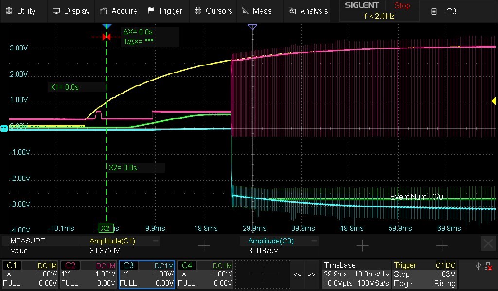
- If I use the enable button on the lab supply, it starts up as expected. 
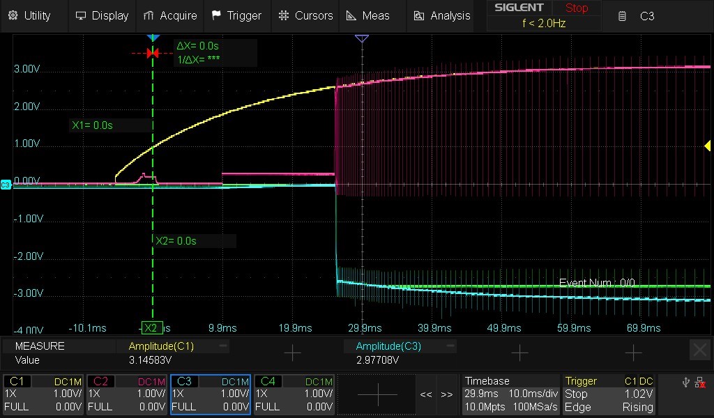
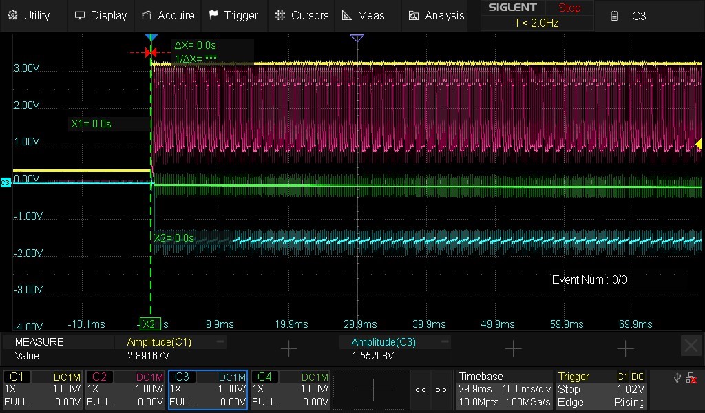
- If I use the jumper connecting VIN (through VDD_NEGRAIL in the schematic), it generates a somewhat wobbly voltage between -200mV and -600mV. It does not recover from this situation unless I cycle the power through the enable button on the lab supply.

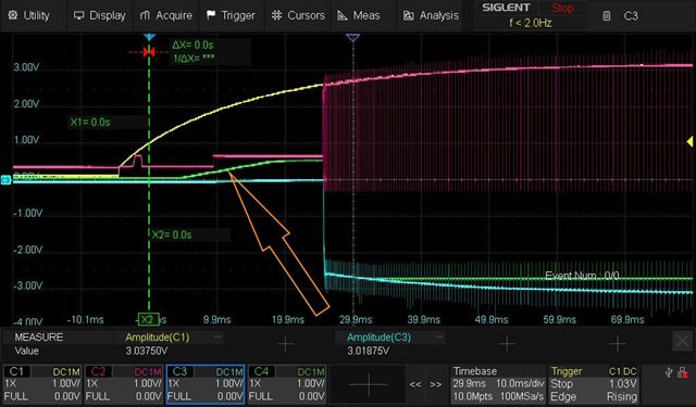
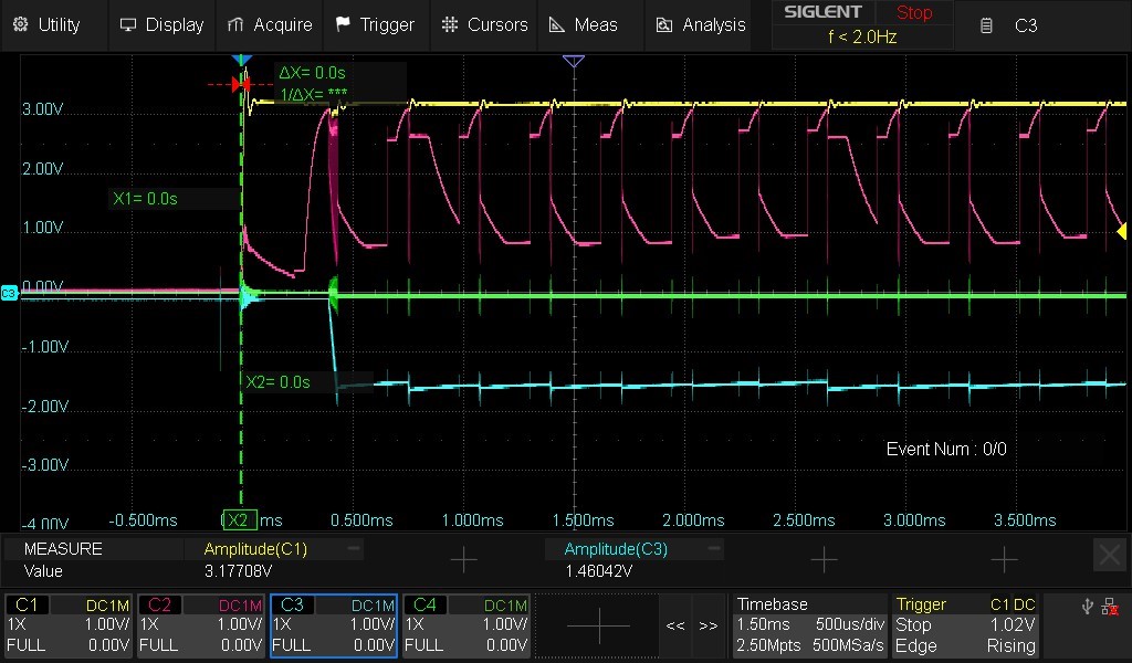
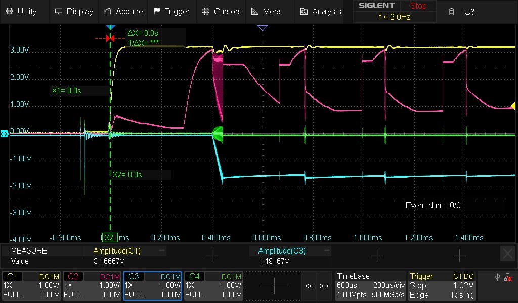
A scope image of the power up event on the VIN pin shows a significant difference on how the voltage rises up on this pin (and I can imagine that this DOES make a difference on the device). 

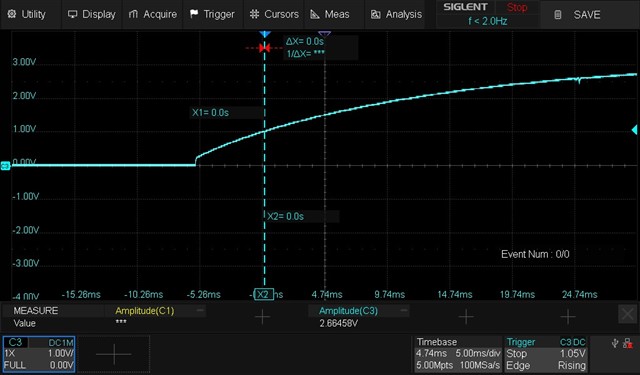
Power up from lab supply


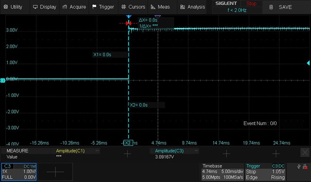
Power up from connecting jumper on VIN


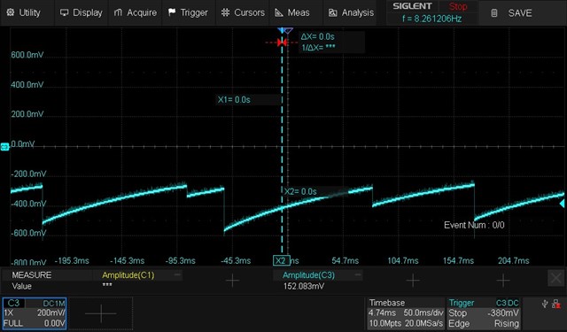
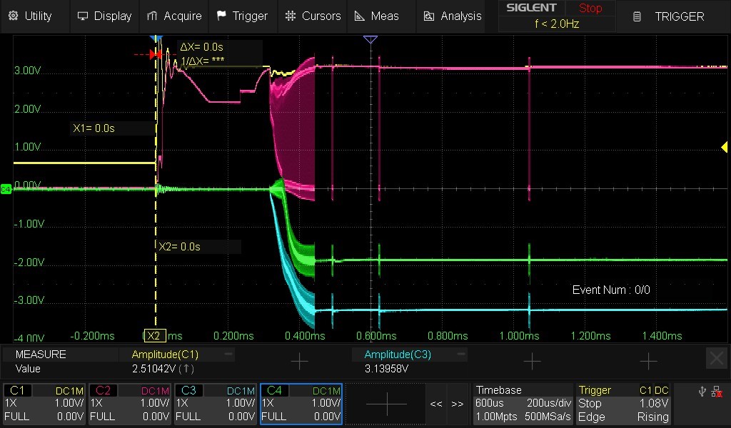
Output when powered up from jumper (power up from lab supply results in normal expected -2.7V output)
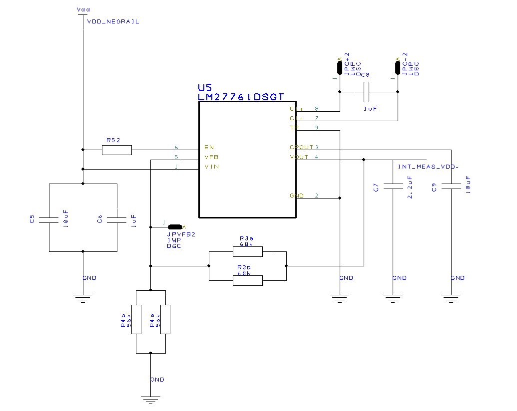

Schematic
(Please note that R4 and R3 are doubled in the design to accomodate for multiple footprints, only 1 of of each is populated. 
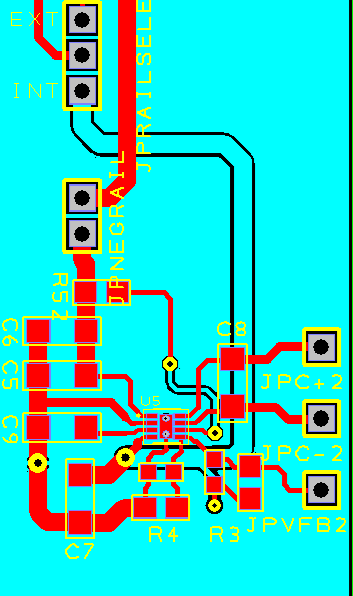
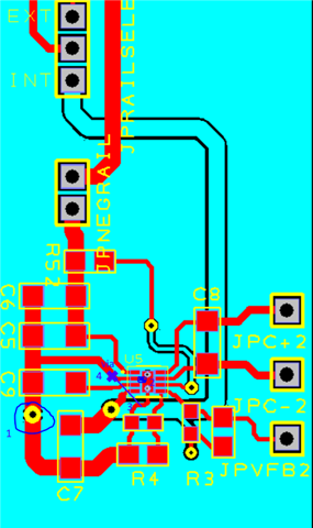
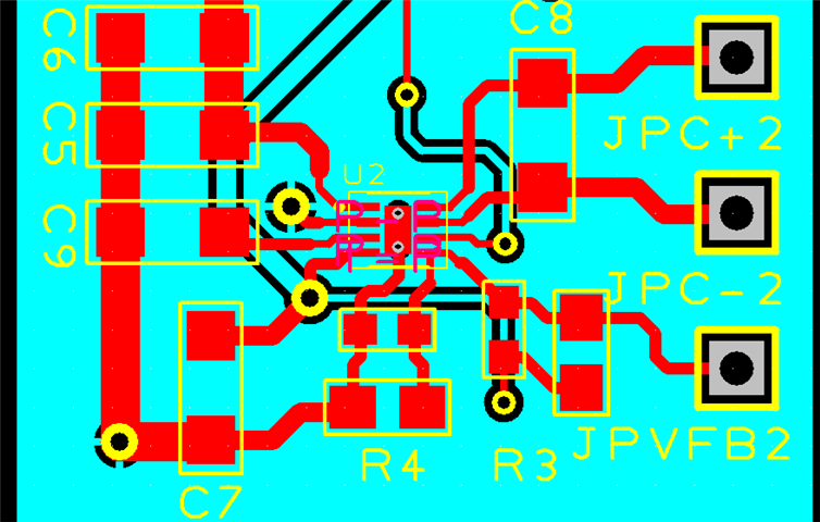
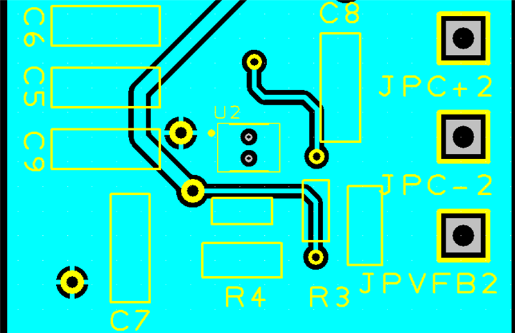
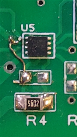

PCB Layout

In my opinion it should work even with the "straight ramp" power up. I have the 27761EVM module that does not have this problem, so it SHOULD be possible to get it correct :-)
The difference between my circuit and that of the EVM is not very big, mainly somewhat different layout directly around the chip and different make of caps and resistors (or so I assume since I don't have P/Ns of what was used on the EVM, but the probability of them being the same is practically zero of course). 

Could it be that I need to use slightly different values for my caps or maybe specific parts?
Maybe there are some issues with the layout that could cause this behaviour?

Any help greatly appreciated!

Martin Koster
Sofrides IO

  • Hi Martin,

    Thanks for using E2E.

    Could you please take a scope shot with VIN, C+ , CPOUT and VOUT plotted together at the fast startup which is failing and the slower one which is passing.

    In addition could you please try out a fast startup without any load.

    Best regards,
    Sepp

  • Hi Josef,

    Thanks for your swift response. Please find below the scope shots:


    Slow start with load.

    Yellow line on top is VIN. Next line at cursor (Magenta) is C+, Cyan line at 0V, lowest one towards the end of the image is CPOUT and finally the green line that is slightly above CPOUT is VOUT. 


    Fast start with load


    Slow start without load


    Fast start without load


    I hope these help to identify the problem. Feel free to get back to me if you need any additional information.

    Kind Regards,

    Martin Koster
    Sofrides IO

  • Hi Martin,

    Thanks for the additional plots.

    • Could you please do the "Fast start without load" plot again with a zoom in at the startup ramp to see the startup in more detail.
    • On the "Slow start with load" plot the VOUT is positive at the ramp phase which is coming somehow from outside because CPOUT is 0V at this time, see plot.
    • Please try to use a Schottky diode at VOUT to cut the positive voltage at startup.

    Best regards,
    Sepp

  • Hi Sepp,

    Please find below the requested plots:


    Fast start without load at 500 us/dev


    Fast start without load at 200 us/dev

    Interesting notion on the VOUT line being positive. I looked at this line with the LM27761 disconnected and at power up, it will float around 0.62 V. There are some OPAMPs behind this rail, so I guess the positive rail is "leaking through" into the negative rail when it's not driven. 

    I am assuming this is not causing the problem we are looking at now, since the situation without load (and thus without undesired VOUT pull) has the same problem.
    - Is that correct?
    - Is it still recommended to put a schottky diode in place in the next revision?

    Kind Regards,

    Martin Koster
    Sofrides IO

  • Hi Martin,

    The LM27761 is very sensitive to a positive Vout at startup in general but this Schottky diode will not solve your problem because we see the fail behavior also without load.

    Have you checked more units/boards or only one?

    Which capacitors you are using? Could you please provide the part numbers.

    Best regards,
    Sepp

  • Hi Sepp,

    Part numbers for the capacitors:

    C5 (VIN) 10uF Samsung CL31B106KAHNNNE
    C6 (VOUT) 1F Samsung CL31B105KBHNNNE
    C7 (VOUT) 2.2uF Samsung CL31B225KBHNNNE
    C8 (C+/C-) 1F Samsung CL31B105KBHNNNE
    C9 (CPOUT) 10uF Samsung CL31B106KAHNNNE

    I just checked another board, it shows exactly the same symptoms (only tested without load).

    Let me know if you need anything else.

    Kind Regards,

    Martin Koster
    Sofrides IO

  • Hi Martin,

    Could you please provide the "Fast start without load at 200 us/dev" plot measured on out TI 27761EVM with the same condition.

    So far everything looks ok on your board....

    Best regards,
    Sepp

  • Hi Sepp,

    Of course, here you go:

    Looks quite different, but then again the EVM does indeed correctly deliver the negative voltage of (in this case) around -1.83V.

    Hope this helps, please keep me posted!

    Kind Regards,

    Martin Koster
    Sofrides IO

  • Hi Martin,

    After a long internal discussion we came to the conclusion that the source for the fail behavior could be the GND connection on your board.

    You have a long trace (high inductance) to connect the GND pin (1) of the device to the GND plain and also to the thermal GND pad.

    So please try to 

    • connect the GND pin to the thermal pad under the device (2)
    • connect the GND pin to the trace which is connected to the thermal pad outside (3)
    • drill a hole and make a via to the GND plain near to the GND pin (4).

    It could be that on the fast startup it will be not solve the issue totally but please try out if this modification improves the behavior. 

    Best regards,
    Sepp


  • Hi Sepp,

    Connection 2 (GND pin to thermal pad under the device) will need a PCB layout change, so that will have to wait until the next revision. Connection 3 I can make with a jumper wire, should be rather easy. For connection 4 I will need to gather some courage to do the drilling, but I will give that a shot. Will update you with results as soon as I have them.

    In the mean time, I did some other testing. An earlier version of this board did have a via pretty much at spot nr 4 (see top copper image). I cannot reproduce the fast startup issue on this board, which suggest (but does not conclusively prove, see next remark) that this via is relevant, if not crucial to this problem.

    This earlier version had different issues though. It ignored the guideline "The returns for both CIN and CCPOUT must come together at one point, as close to the GND pin as possible" (data sheet, section 10.1). The negative output voltage of this version, would often be unstable and heavily depend on the input voltage. After double checking on the datasheet, I realised my omission on the returns of CIN and CCPOUT. They would feed back to pin 2 via the ground plane only and also through a via that is far away and with another track lying in the way, making the path very very long (see picture with bottom copper). I temporarily fixed this with a soldered wire from the GND side of CIN to the GND pin. After this, output voltage was perfectly stable. In the next revision I fixed this in the layout, but deleted the via near the GND pin. In hindsight, maybe that wasn't such a good idea...

    What strikes me as odd in this, is that there is a small mistake in the older design: the two vias in the thermal pad are not actually connected to the ground plane (again, see image of bottom copper layer). Nevertheless the via connecting the GND pin to the ground plane does seem to make a difference...

    I hope this extra information is of use and does not add to the confusion :-)

    I will get back to you as soon as I've evaluated the PCB changes.

    Kind Regards,

    Martin Koster
    Sofrides IO


    Earlier version top copper (and bottom copper underneath)


    Earlier version, bottom copper

  • Hi again,

    First result is in. I have done what must be the ugliest fix in PCB development history with a strand of wire soldered to a part of the track coming from the GND pin (solder mask scratched clean) to the connection point of the VFB resistor where it is connected to the thermal pad. See picture (and laugh). 

    This improves the situation considerably. It now starts up quite consistently at a fast startup without load. The only discrepancy I notice is that --sometimes-- it rises up to an output voltage that is about 2-3 mV lower than the intended (set) output voltage. In concreto, sometimes it starts up and stabilizes at 2.699V while normally it starts up to 2.702V. This does not seem to happen on a slow startup. That is still a bit fishy, but as said, really a lot better, so we may be on the right track here.

    I think I've used up my luck for today and will save the via drilling operation for tomorrow.

    Kind Regards,

    Martin Koster
    Sofrides IO

  • Hi Martin,

    Thanks a lot for the good news. Let's wait until tomorrow for the next results.

    Best regards,
    Sepp

  • Hi Sepp,

    Managed to make a via without ruining the PCB :-)

    I've tested with three different options:

    1. Jumper wire from GND pin to thermal pad (picture from yesterday)
    2. Via from GND pin to GND plane at bottom copper, #4 in your picture from Aug 19th.
    3. Combination of 1 and 2

    The original instability problem with VOUT not getting beyond -600 mV is no longer visible in all cases. In that respect: BIG SUCCESS!

    Like yesterday, I've observed that sometimes, the output stabilizes at 2.699V while normally it stabilizes at 2.702V. With either option 1 or 2, this seems to happen around 1 out of 10 times. 
    With option 3, this still happens, but very rarely to the point of being dificult to reproduce.

    Any idea what is going on here? Should we be worried about this?

    Kind Regards,

    Martin Koster
    Sofrides IO

  • Hi Martin,

    Thanks a lot for your feedback. In general you should place vias on every GND connection of each component to the GND plain to get a good grounding.

    You should not worried about this. I think after a good grounding you won't see it.

    Best regards,
    Sepp 

  • Hi Sepp,

    Thanks very much, I will take that into account for the next revision. Is it OK to leave this thread open and let you guys review the updated layout when it's ready? (Will be a week or two)

    Also: is a PCB track implementation of the jumper wire (option 3 in your picture, from ground pin to the thermal pad track south of the device) still necessary when GND pin pad is connected to the TP under the device? Because this track is very difficult to lay down with all the Cs and the feedback resistor in the way and it seems to me it doesn't really add anything once the connection under the device is present.

    Thanks ahead for your advice!

    Kind Regards,

    Martin Koster
    Sofrides IO

  • Hi Martin,

    Option 3 was only for testing means improve the grounding afterwards. It's not necessary at your new improved layout.

    I will close this threat now because I'm out for 3 weeks, so please create a new one if you are ready with your new layout.

    Best regards,
    Sepp

  • Hi Sepp,

    Allright, will do! Thanks for your help and enjoy your time off!

    Kind Regards,

    Martin Koster
    Sofrides IO