Hi,
I do not have access to the BQ I2C and USB2ANY tool to see what the status of the charger is.
However, what I can say, is that in sink mode, the STAT LED turns on (no flickering or blinking or anything), and in source mode, it doesn't. The STAT LED turns on whether the sink voltage is 20V and it doesn't actually work (drawing 0W) or the sink voltage is 12V, and it does work (drawing ~19W).
The battery is made of just standard 18650 Li-ions (2.5 - 4.2V/cell), so 11V = 3.67V/cell = about 60% SoC probably.
Yes, I am also suspecting it is an issue with the firmware configuration, and what commands the BQ is being sent potentially.
My firmware flashing sequence is as follows:
1. Generate the full flash binary
2. Convert it into a .c header file using xxd in Git Bash
3. Use an Arduino microcontroller to load the firmware onto the device, which provides output to the serial monitor when flashing is complete and double-checks whether it flashed correctly after each bit.
What I am wondering is whether I have an issue with my firmware flashing sequence, or the firmware generation has an issue itself. Let me know which other details you want me to provide so we can solve this problem.
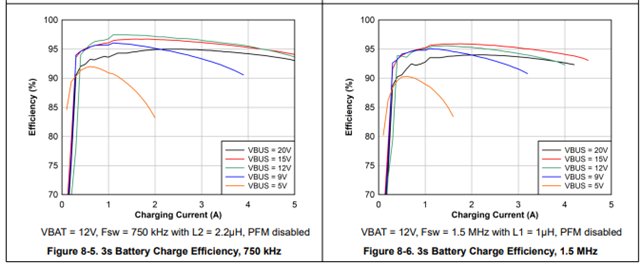
One thing I did notice is that I'm trying to charge a battery at 4.5A up to 12.45V from a 20V power supply, which is beyond the graphs of the charging current vs efficiency vs input voltage figure in BQ25798 datasheet. Could it be hitting some sort of internal limit at these power levels, even though, as of the moment, 11V*4.5A = 49.5W (which is still way below the 60W budget)?
Thank you.