This thread has been locked.

If you have a related question, please click the "Ask a related question" button in the top right corner. The newly created question will be automatically linked to this question.

BQ79631-Q1: Negative Differential Readings on Link+/Link– and Charge+/Charge–

Part Number: BQ79631-Q1

Tool/software:

Hi ,

I’ve designed a board using the BQ79631 with the schematic exactly as shown in the datasheet. The device powers up fine, and I’m able to read correct values for HV+ (Battery +) and Fuse+. Below are my measured differential readings (in volts):


VS1 = 0.012 V (Dev 1 Cell 1) → Floating

Battery+:

  • VS2 = 4.978 V (Dev 1 Cell 2) → VS2 / TSREF

  • VS3 = 2.416 V (Dev 1 Cell 3) → VS3 (HV +)
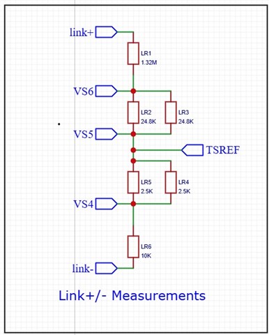
Link+/Link–:

  • VS4 = –4.115 V (Dev 1 Cell 4)

  • VS5 = 1.693 V (Dev 1 Cell 5) → VS5 / TSREF

  • VS6 = –0.017 V (Dev 1 Cell 6)

Charge+/Charge–:

  • VS7 = –1.684 V (Dev 1 Cell 7)

  • VS8 = 1.699 V (Dev 1 Cell 8) → VS8 / TSREF

  • VS9 = –0.013 V (Dev 1 Cell 9)

Fuse+:

  • VS10 = 0.012 V (Dev 1 Cell 10) → VS10 / TSREF

  • VS11 = 2.440 V (Dev 1 Cell 11) → VS11 (Fuse +)

Unused:

  • VS12 = 4.556 V

  • VS13 = –0.000 V

  • VS14 = –0.001 V

  • VS15 = –0.001 V

  • VS16 = –0.001 V


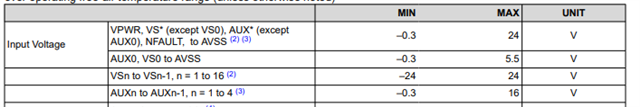
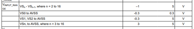
According to the datasheet, for a correct differential measurement:

  • VSn – VSn-1 should be between –1 V and 5 V

  • Also, VSn > VSn-1

However, with the datasheet-recommended resistor ladder configuration, I can’t see how this is possible — especially since VS2 is referenced to TSREF (as are VS5, VS8, and VS10). This makes it impossible to maintain VS10 > VS8 > VS5 > VS2 in practice.

Because I’m seeing negative readings on some channels (particularly for Charge+/Charge– and Link+/Link–), I’m concerned that:

  1. The IC could be damaged over time.

  2. It may never be able to measure these points correctly.

I’ve attached my resistor ladder schematic for reference. Any suggestions or clarifications would be appreciated.

Thanks in advance!

  • Mounish,

    Where to you see the requirement that Vcn > Vcn-1? The only requirements I see are those in the device electrical characteristics where the absolute maximum ratings are thusly:

    and the recommended operating conditions are:

    Provided that your Vcn pins are within these ranges there should be no damage to the device.

    Regards,

    Bo

  • So,

    Is a negative voltage acceptable? I got 

    Link+/Link–:

    • VS4 = –4.115 V (Dev 1 Cell 4)

    • VS5 = 1.693 V (Dev 1 Cell 5) → VS5 / TSREF

    • VS6 = –0.017 V (Dev 1 Cell 6) 

    1.How to use this data to calculate Link+ and Link- Voltage?

    2. Clear VS pin voltages are out of recommended value range

    3. To read Positive Voltages, we have to maintain this Vcn > Vcn-1 right?

    Please suggest

    Thanks & Regards

    Mounish

  • Mounish,

    Any voltages outside of the spec are not okay and could cause damage to the device. So, the reading of -4.115V is not acceptable. 

    1)

    You can find our guide to calculating LINK+/- in section 9.2.1.2.3 of the datasheet. The following sections also have information on the other measurements you are taking. However, LINK- is supposed to be similar to the ground voltage (near zero) and LINK+ is supposed to be near the total pack voltage. From the reading you have of VS4 (-4.115 V) and VS6 (-0.017) it seems like you have significant leakage current in your system or some other more pressing issue.   

    This diagram in section 9.2.1 of the datasheet should give you a good idea on what the pins should be connected to:

    2)

    I do not understand what you are asking here. You should not have VS pins outside of the recommended value range.

    3) 

    Not as far as I can tell. 

    Regards,

    Bo

  • Hi Bo,

    Can you please check if there are any mistakes in the schematic? For your information, I have used the same reference to design the PCB. Please find attachment of my schematics?Schematic_Bq79631-BJB-V1_2025-08-13.pdf

  • Hi BO,

    Can you please check..I am waiting for your reply

    Thanks&Regards

    Mounish

  • Mounish,

    If you measure the TSREF pin, what voltage do you see?

    Regards,

    Bo

  • Hi BO,

    Sorry for the delayed response.

    I’ve noticed that when no external measurements are connected, TSREF reads 4.9V. However, its value keeps changing whenever input measurement voltages are applied.

    My concern is that since TSREF is supposed to act as a reference voltage, it should remain stable and not vary with the input. This makes me think something might be wrong.

    Could you please advise?

    Thanks&Regards

    Mounish