Tool/software:
Dear Expert
There are two specifications in the lM5017 specification sheet that need your help to clarify or assess the risks
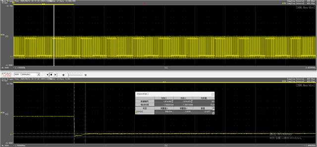
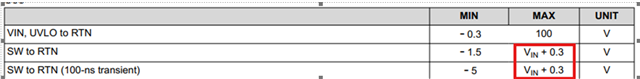
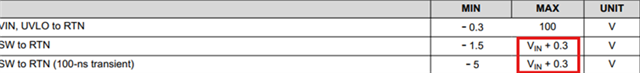
1) The Max specification of SW-RTN is limited to Vin+0.3V. We measured a Spike with Vin+1V (Vin=13.2V) during light load, please help evaluate if there is any risk associated with this.
(My understanding of the Max specification for SW-RTN is that the conduction voltage drop of the upper diode will clamp the SW-RTN to Vin+0.3V. The specification sheet provides a theoretical clamp value, not necessarily lower than this value.)
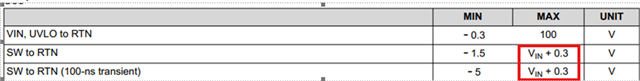
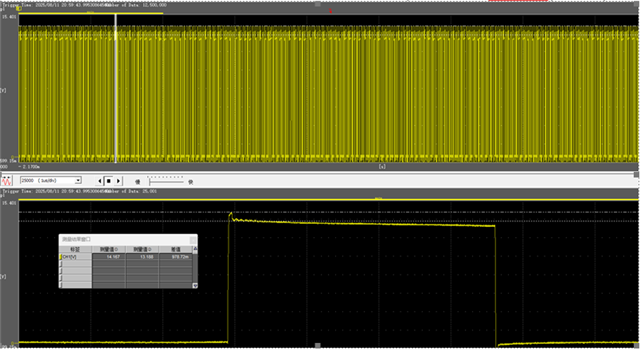
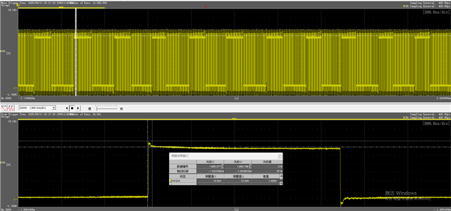
2) Does the SW Vin specification (MOS stress) need to be reviewed. There is no restriction on this item in the specification sheet. Do we need to refer to SW-RTN to review the positive and negative voltage? We will measure it ourselves -2.1V@73ns of
Negative Spike, and+ 1.4V@87ns The positive Spike;
Please help evaluate whether there are risks associated with the positive or negative specification of SW Vin, how it is considered, and whether it needs to be reviewed with reference to SW-RTN.