TPS23731: Questions/Ideas related to using UCC24612 or similar device instead of full range CCM flyback using extra transformer winding

Part Number: TPS23731
Other Parts Discussed in Thread: PMP22806, , UCC24612

Tool/software:

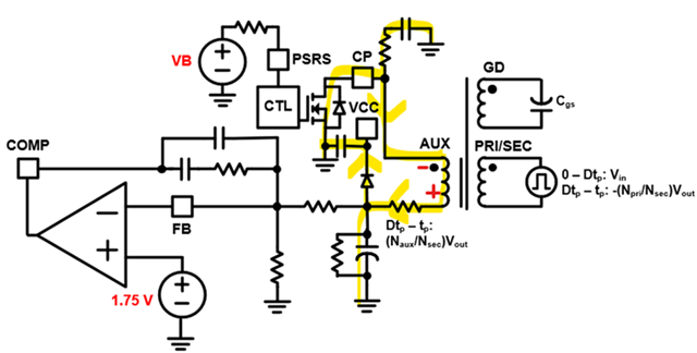
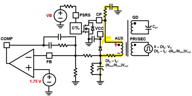
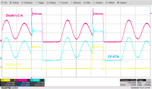
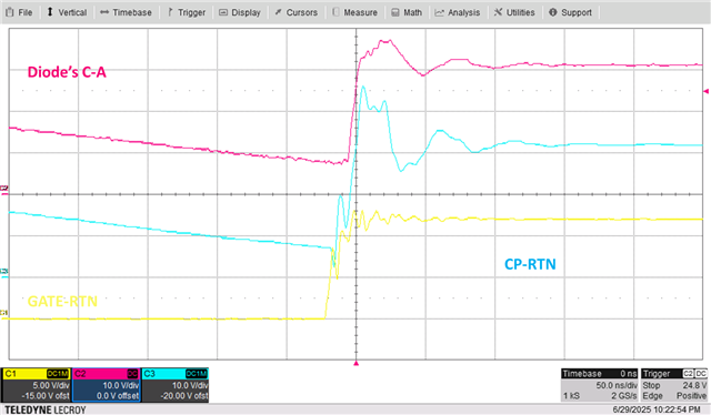
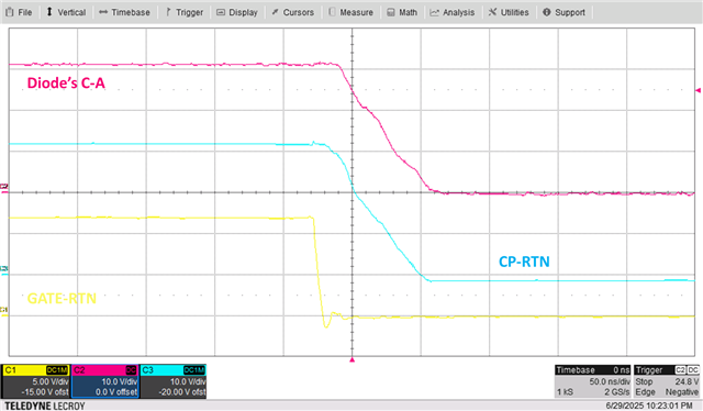
In the related thread (original question), I have questioned whether " actively cancelling (through the use of CP output) the leading-edge voltage overshoot (causing the feedback capacitor to peak-charge)" can be truly postulated. Because the body diode conducts immediately as soon as the primary Mosfet is switched off and the leakage inductance spike is thus exposed to the feedback capacitor. But there is a sort of corollary: only if there would be a small delay of the CP-Mosfet being switched on, until that, the nominal winding voltage does not inject current to the capacitor because in the previous cycle the capacitor is charged with the winding voltage during primary switch off-state minus the minimal voltage drop over the "ideal diode" behind the CP terminal. On the start of the next cycle, only the body diode conducts and because the capacitor has not dropped the voltage more than a few mV, the net voltage "available" to the capacitor is lower: winding voltage minus body diode. So in this minimal time interval, the leakage inductance spike may inject some current (limited by the series resistor), but it has no effect. And hence the capacitor voltage is quite accurately sensing the net winding voltage.

But according to my experiments, it seems that any delay at all is hardly detectable. Perhaps any TI-employee could give a specification of it. Of course, a delay should be longer than the spike width in order to obtain best load regulation.

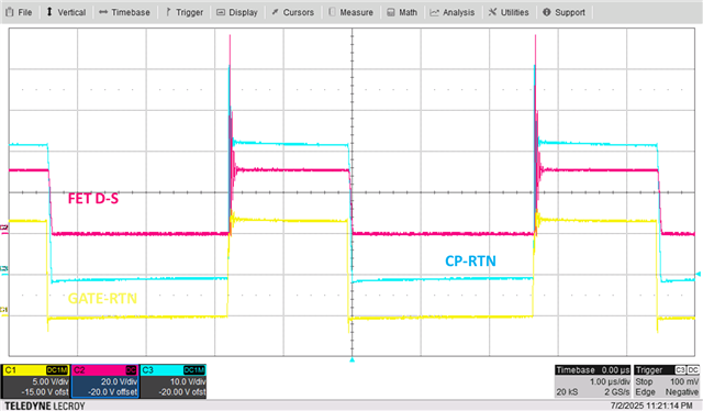
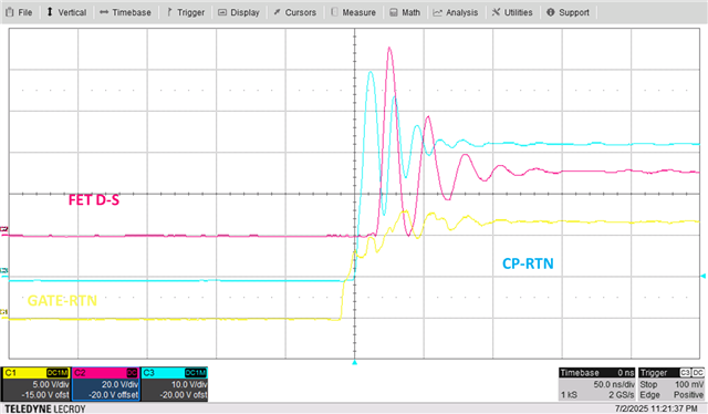
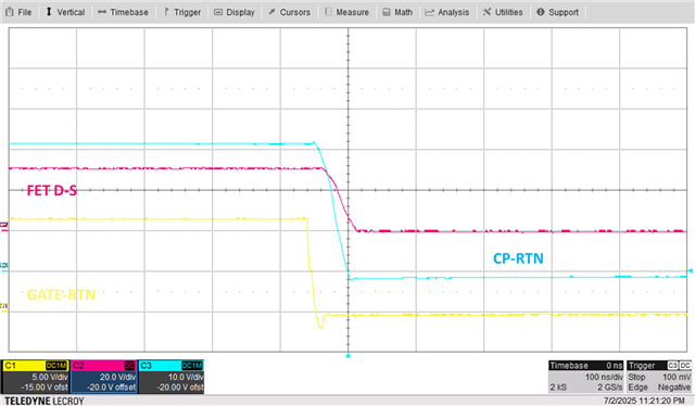
The explanation above could also help in getting a good load regulation also if an ideal diode circuit on the secondary is used as rectifier. The output voltage is (ideally) based on the regulation of the secondary winding voltage when the Mosfet of the ideal diode circuit conducts. But during an initial delay (of say 40 ns) before the Mosfet is switched off, the secondary winding voltage is then approx. 0.6V higher. This would be reflected in the aux (and the primary) winding. And that would well increase the feedback capacitor voltage (effectively lowering the output voltage). But if the CP-Mosfet would also have a delay of no less than the secondary side delay, this effect would actually be neutralized.

So even more it is interesting to know the CP-Mosfet on-delay.

Next question: could a timed control signal applied to PSRS force an extra CP-Mosfet delay? And even a premature stop of CP Mosfet conducting when the voltage on PSRS is set to low? In short: a signal that follows the CP-voltage, with offset shift towards the positive voltage range and a delay onto the positive slope on PSRS. To say it simple: can PSRS be "modulated" by a digital signal or would a built in flip-flop behind PSRS make a continuous digital control impossible?

  • Hi Rob,

    Thanks for reaching out.

    Normally a flyback + PSR + diode rectification (including ideal diode case) combination does not have a good load regulation. Since the Vout sampling signal is based on AUX winding not the Vout directly. Changing to SSR will solve the major issue of load regulation. But if keeping PSE, changing diode rectification to sync FET will improve the load regulation too, but not as significant as SSR.

    For your concerns of transient ripples, when primary FET is off (D x t_p to t_p), current can flow out from CP pin either from its FET's channel or body diode. Vout sampling cap will be charged at this time. Inrush by leakage/stary inductance can be absorbed by VCC cap and RC snubber. 

    When primary FET is on (0 to D x t_p), CP pin has a positive voltage bias, inrush by leakage/stary inductance can be absorbed by RC snubber. 

    Best regards,

    Diang

  • Thanks for your answer, Diang. However that adds no new information for me. Please answer whether the PSRS pin may be sourced by a digital level square wave in order to exactly limit the time interval that the CP-Mosfet is conducting. I don't guess that I'm going to implement such, but at this time I also cannot exclude this. Because of TI's exact knowledge of the internal circuit, an answer to this question can be given, at any case by the design engineering section.

    The same applies to the delay in ns of CP gate drive on after the main MOSfet gate has switched off. It should be possible to specify this.

  • Hi Rob,

    Thanks for your reply. I will get back to you in 3 business days.

    Best regards,

    Diang

  • Hi Rob,

    Sorry that some of design information is nondisclosure. From application aspect, we provided the design recommend: to make CP works properly in flyback, PSRS open for sync FET, PSRS short to RTN for other cases. Ideal diode is not the same with sync FET as we already discussed. 

    Could you share the full PoE + DC/DC circuit schematic so we can check the details?

    Best regards,

    Diang

  • What I ask has nothing to do with design information, but with behaviour. Which could simply be measured (CP-Mosfet ON-delay) and verified (modulation via PSRS) by setting up an appropriate test-setup.

    Note: Ideal diode tests are - of course - only executed with PSRS to RTN.

  • Hi Rob,

    Hope below waveform behavior can help. 

    Best regards,

    Diang

  • Thanks for presenting these oscillograms, assumed to have been recorded using the EVM as is, where PSRS is tied to RTN. I guess that "Diode's C-A" means secondary side diode, in the assumed case the secondary side mosfet exhibiting no delay except slew. Since the blue line does not  go below the trace reference (sec. GND), the mosfet seems immediately on because no short diode conduction time is visible (as would be the case by using UCC26412). Using a lower V/div. setting, one would presumably see a small negative voltage.

    Contrary, the CP to RTN clearly has a negative voltage of approx. -1V which shows that the CP-Mosfet is not switched on (due to PSRS tied to RTN). Of course no switching delay is visible. In the case of PSRS open, one could  see a short time that approx. -1V is seen, followed by - let's say - 0.1 V because of Mosfet on. But in practice, I see no such delay. That also means that the leakage inductance spike is by no means absorbed by "a unique approach which basically consists in actively cancelling (through the use of CP output) the leading-edge voltage overshoot" (datasheet 8.3.6.3). This is why you need a small resistor between the aux winding and the 3.3uF feedback capacitor. An oscillogram of the voltage on the winding side of this resistor should show this (could you supply this? I don't have the EVM). Despite this, regulation can work in a reasonably good way, because in CCM, the spike energy increases less with increasing power in CCM than in DCM mode.

    I think it's up to you to prove whether the quoted statement from the datasheet is correct or not.

    Edit: with PSRS tied to RTN on EVM with any else unchanged, I'd expect a higher output voltage, since the voltage on the feedback capacitor is regulated (fixed voltage), while the amplitude of the aux winding is increased by the difference of CP-Mosfet drain-source voltage in conduction state and its mere body diode voltage. This increase is reflected on the output winding.

  • Hi Rob,

    Thanks for your reply. I will get back to you by this week.

    Best regards,

    Diang

  • Hi Rob,

    Thanks for your patience. I think we could merge our discussion on another similar thread. 

    The waveform is captured by TI's reference board. This board has shorted PSRS to RTN (you can also use schottky at RTN to replace CP's FET in this case when no PSR sync FET). 

    Also please check this case when PSRS is open. I saw the CP is closer to RTN but not too much, may be the CP FET is high on-resistance. 

    Best regards,

    Diang

  • Hi Diang,

    It looks that you're applying approx. 20V input voltage and hence, use the separate DC input. It would be interesting to execute the same measurement also when PSRS is left open as is originally the case on the EVM. Supposed there is some delay between Drain from 0 to positive voltage  and CP Mosfet on. In that case, the negative voltage would then measure approx. -1 V, because only the body diode would conduct. Supposed then that the CP on delay would be 100 ns, then this -1 V could be seen for that time, and than immediately get close to 0V, as outlined in my previous posting entry. Then, part of the leakage induction spike would indeed be compensated as stated in the datasheet.

    BTW: the very high spike you measure, followed by ringing, is apparently due to applying a scope probe with the standard GND wire instead of using the GND ring close to the probe tip, that facilitates the shortest possible GND route.

    EDIT - corollary: Because of the facts that the output voltage is quite constant over time and this also applies to the voltage of the (for an aux supply relative) big - 3,3µF - voltage over the Feedback capacitor, the picture is a bit more complex, since then the voltage over the winding (during on-state for aux and output) is also constant. Consequently, the negative voltage could NOT reach -1V in the first (assumed) 100 ns after the primary Mosfet is switched off. During this small time interval, the auxiliary winding current would be approx. zero. So, I think that a better way to know if there is a CP on delay is to measure the current through the resistor between Aux winding and feedback capacitor! But the presence of a spike may well be visible as a short negative excursion in the case CP is just in off state because of a minor delay of its internal gate control. Such a negative spike related excursion would inherently limit the injection into the feedback capacitor.

    EDIT 2 (afterwards I get aware that the oscillograms above were done on the PMP22806 reference design with secondary simple diode rectification). Therefore I put some strikethrough formatting above.

  • Hi Rob,

    Thanks for your reply. I will get back to you in 2-4 business days.

    Best regards,

    Diang

  • Hi Rob,

    Thanks for your patience. 

    The input voltage for both TPS23731 + sync FET and TPS23731 + diode are the same. But they are boards with different DC/DC.  

    My understanding is the delay of the CP's inner FET, as well as the delay is within a certain time and not influence the switching period, may not be significant for the regulation for sync FET case. Since even the CP's inner FET is off, the current can flow through the body diode and only may influence ~0.7V difference in regulation. PSR normally has a poor regulation compared to SSR so the ~0.7V difference may not be a big concern.   

    Best regards,

    Diang

  • Hi Rob,

    We considered the max rating as it may cause permanent damage to the device as the datasheet mentioned but not absolutely will cause damage. From application aspect, we provided the design recommend: to make CP works properly in flyback, PSRS open for sync FET, PSRS short to RTN for other cases. From my experience, I had not seen other cases that CP was damaged when the CP & PSRS circuits were configured correctly.  

    Sorry that I could not give other comments about this CP pin configuration. I think we have good understanding of FET's 3rd quadrant operating and I had gave the operating diagram of this pin. Let me know if you have other concerns or questions.

    Best regards,

    Diang

  • I have started to execute measurements of the voltage across the resistor that is present between aux winding and the Feedback voltage buffer capacitor, as suggested in a posting above:

    So, I think that a better way to know if there is a CP on delay is to measure the current through the resistor between Aux winding and feedback capacitor!

    Measurements executed this way appeared not to show a clear CP delay as hoped, but then I had the idea to interrupt the copper trace between CP and the other components that were tied to CP and then connect the then open end of  the aux winding to an extra diode (ES1JFL). CP has then become a pull-up resistor of 1 kΩ to VB pin (5V). The result: there is a delay of 120 ns between primary side switch on to off state (as measured at the aux winding end that is connected to the extra diode inserted into the circuit) and the slope of CP from non-conduct to conduct state (low):

    Ch 1 = cathode of separate fast standard diode (is also connected to aux winding end normally connected to CP)
    Ch 2 = CP signal, as tied via 1 kΩ to VB

    Cursor Y2 represents the voltage across the feedback capacitor. The extra diode indirectly shows the high current induced by the spike (where it must be noted that ES1JFL has approx. 1.6V Vf at 0,75A, which is the approx. spike peak current).

    Conclusion:

    1. Due to the delay, spike energy that is contributing to the voltage of the feedback capacitor should be reduced, but its effect is limited because of the body diode that conducts always in the application circuit and limits the amount of energy. The mechanism as advertised in the datasheet of the TPS23731 exists, but not in the sense of "consists in actively cancelling" the leading-edge voltage overshoot.
    2. Having stated that, a fairly good load regulation can also be achieved using a UCC24612 as a secondary rectifier as long as its delay from detection of switch transition to output current flow to the SR-Mosfet is shorter than the CP delay. The UCC24612-1 fulfills this requirement, but the (used) -2 suffix version not. The reason: in the latter case, a SR-Mosfet that is not yet conducting will exhibit a larger winding voltage because the output voltage changes very slowly for each PWM period due to the capacitor bank. This voltage is reflected to the aux winding too, and would lead to extra feedback capacitor charging when CP would be conducting at that time.

    Regarding the second list entry it must be said that the beneficial delay arrangement as outlined only applies if PSRS is not tied to RTN. That also meant that the secondary side rectifier must behave as a full load range CCM, because otherwise the AUX winding is forced to deplete the transformer energy via a conducting CP also in reverse current direction (to CP inside chip that would also discharge the feedback capacitor somewhat).

    In a subsequent posting I'll show the results of current measurements from the winding to the feedback capacitor (see text on start of this single posting).

  • I have reported the posting above "We considered..." as abusive. But there appears no dialog about that, so I comment the reason via reply (which may be deleted): It is not strictly abusive, but redundant, because exactly the same text appears in the other thread related to damages on the CP functionality: e2e.ti.com/.../5979931

  • According to my announcement in the previous post, aux current measurements are presented here. In order to have better resolution, I have increased the series resistor to 6R8. In my design, the feedback capacitor is 4µ7 while its parallel resistor is 2k0.

    In order to prevent CCM-conflicts in PSRS open input mode (CP output according to full range CCM; secondary UCC24612-circuit as ideal diode), the power level is chosen to have CCM also on the secondary side.

    Here when PSRS=0 (CP-Mosfet not active). Both traces are referred to the feedback voltage (11.4V). Therefore, an Y-cursor is set to -11.4V in order to judge the plain voltage of CP referred to RTN.
    Trace 1 is CP-voltage and Trace 2 is voltage on winding side of the 6R8 resistor. Here, the GND-ring of the probe tip is directly connected to the reference voltage in order to minimize ringing effects caused by the standard GND-wire with its connecting clip). The V/div. is chosen to have an excursion of the spike just below the upper screen limit, in order to have better resolution of the current curve after the peak ends. It peaks at approx. 5.3V which means: 0.78A (using transformer from Pulse PA3855.002NL).

    After the spike ends, no noticeable current flows through the resistor: 1/10th div is 0,16V (24 mA - which is expected to be somewhat over the average current that flows from the feedback capacitor into the DC/DC-circuit and its parallel resistor). In this case that means that the spike delivers too much energy, because good regulation requires that energy must be transferred mainly after the spike until the primary MOSfet is switched on.

    Next, the current is shown when PSRS is open. It can clearly be seen that CP voltage is approx 0 V due to the MOSfet switched on. In this case, we can clearly see a current through the winding after the spike is elapsed. But it goes through zero and reverses direction (discharge feedback capacitor) until the primary MOSfet is switched on. Thinking about this, I conclude that this behaviour is related to the CP voltage quite clearly kept at 0V. Within a switching cycle, it is normal that the winding voltage is not necessarily constant. It may drop a bit during linear drop of output winding current. This explains the current curve through the winding and hence, the 6R8 resistor.

    In both oscillograms, I have determined a possible CP on delay time as 170 ns. Which cannot really be determined. Moreover, the delay of the ideal diode on the output may interfere with the curves measured, and hence, I decided to determine CP delay simply directly, with simple diode SR.

    Generic Note

    In former projects, I successfully realized PSR-circuits with inductor or small series resistor in the aux winding path. However, this is the first time that I analyze this using current measurements. Which represents a perfect way to judge whether the design is correctly dimensioned or not: a noticeable net positive current (after the spike) must be visible. In this case varying spike energy would hardly affect the regulation.

    Just some thoughts: an inductor (instead of series resistor) has the advantage of representing a higher impedance for the spike, and allows the spike to become higher (and shorter in time). The spike may then also have less energy when the inductor indirectly forces spike energy to seek "outlet" in another winding. But an inductor has the disadvantage that it stores the spike energy - which will then be released to the feedback capacitor (after the spike). A resistor is beneficial because it does dissipate a part of the energy.

    A few weeks ago, I experimented with a combination of R and L (in parallel). I achieved the best load regulation when L = 4.7 µH and R = 20 ohms (compared to 3.3 Ω only).

  • Hi Rob,

    Thanks for your reply. I will look into it and get back to you in 2-5 business days.

    Best regards,

    Diang

  • Hi Rob,

    Thanks for your patience. 

    It seems that you had done meaningful tests and I believe you have a good understanding of the function of primary side regulation and CP pin with the waveforms from both sides.  

    I will close this thread for now. Please reply or open a new thread if you have further questions or concerns.

    Best regards,

    Diang

  • In short, you get an update (some illness time has passed)

  • Hi Rob,

    Yes and thanks for your patience. 

    Best regards,

    Diang