TPS543C20A:TPS543C20A V_SYS_PWR Circuit Issue (PG Threshold and RSP/RSN Wiring)

Part Number: TPS543C20A
Other Parts Discussed in Thread: TPS543B20, TPS543C20

Tool/software:

  1. PG Threshold Issue:

    • Product Used: TPS543C20A

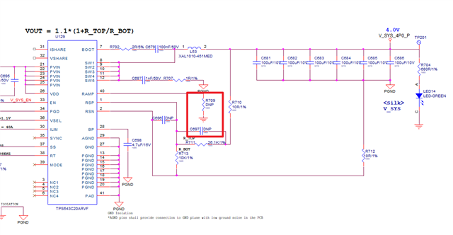
    • Set VOUT: 4V (Based on actual schematic, it is 3.971V)

    • Problem Description: When the VOUT drops by approximately 5% to 3.8V due to load fluctuations, the PG (Power Good) signal goes low.

    • Question: What is the reason for the PG activating at -5% instead of the datasheet's specified -10% Undervoltage threshold, and what modifications are needed to adjust it to -12%?

  2. RSP/RSN Wiring Application:

    • Wiring Application: RSP (Remote Sense Positive) and RSN (Remote Sense Negative) pins were routed with a 100-ohm differential impedance, resulting in thin traces.

    • Question: Can this wiring design cause a misreading of the PG Undervoltage? Please provide guidelines on how to modify the wiring for a more stable design.

  • Schematic: Please refer to the attached schematic (TPS543C20A.pdf). (R_TOP=26.1kΩ, R_BOT=10kΩ)

  • File: The TPS543B20_TPS543C20A_TPS543C20_Calculator-231113.xlsx file was also referenced.

  • VREF: VREF is set to 1.1V.

  TOP : RSP, RSN 

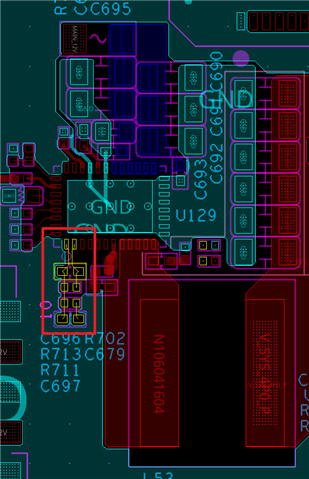
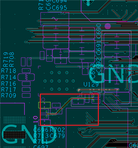
  Regarding R713 and R711 Wiring on Inner Layers

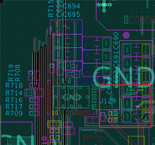
 Regarding R710, R712, and VOUT Cap Connections

7416.TPS543C20A.pdf

TPS543B20_TPS543C20A_TPS543C20_Calculator-231113.xlsx

  •    

    Question: What is the reason for the PG activating at -5% instead of the datasheet's specified -10% Undervoltage threshold, and what modifications are needed to adjust it to -12%?

    The reason PGOOD is responding to less output voltage change is C697.  This "Feed-forward Capacitor" couples high-frequency changes to Vout directly to the RSP pin.  Since PGOOD responds to the voltage at the RSP pin, relative to the reference voltage, this can change the threshold proportionally to the feedback divider R711 / R713 

    At low frequency, R711 / R713 reduce the output voltage by 10k / (10k + 26.1k) = 1 / 3.61

    At higher frequencies, the 560pF capacitor has less impedance than the 26.1k resistor, so the divider attenuates Vout changes less.

    For example, at 50kHz the 560pF capacitor has an impedance of 5.68kΩ and the divider is 10k / (10k + 5.68 // 26.1k) or  1 / 1.47, to twice as much of the change in Vout is reaching the RSP pin.

    The PGOOD threshold is 8-15% of Vref at the RSP pin, or 88 to 176mV on a 1.1V reference.  At 50kHz, that could trigger as low as 130mV on Vout - just 3.2% of 3.971

    what modifications are needed to adjust it to -12%?

    The specified PGOOD threshold is 8% to 16% with a 12% nominal, so you can get the nominal to 12% by removing the C697 feed-forward capacitor, but some devices may still trigger lower than 12%.

    If you are going to remove the Feedforward capacitor, I would recommend also removing the RAMP programming resistor R709.  While this wont fully restore the gain loss by the feedforward capacitor, it will restore most of it. 

    I have attached the updated design spreadsheet to reflect those changes.

    TPS543B20_TPS543C20A_TPS543C20_Calculator-20250814.xlsx

  • I would like to confirm the following points regarding the recent recommendation to remove C697 and R709 in order to adjust the PGOOD threshold:

    1. If C697 and R709 are simply marked as DNP on the schematic, is it sufficient for verification purposes, or would additional modifications be required?

    2. When RAMP is left OPEN, does this correspond to tying it to AGND internally?

    3. For the RSP/RSN routing, is it acceptable not to design them as 100 Ω differential impedance (Outer layer: 0.08 / 0.145 mm, Inner layer: 0.04 / 0.12 mm)?

    4. Would it be better practice to design the RSP/RSN traces with a width of 0.25 mm instead?

    I would appreciate your confirmation on the above points.

    Best regards,

  • If C697 and R709 are simply marked as DNP on the schematic, is it sufficient for verification purposes, or would additional modifications be required?

    Any boards which have already been built would need the resistors placed on the board removed.

    For future boards, you should follow what every your company or contract manufacturer requires to ensure the parts are not populated on the boards.  I do not know your internal processes, so I can't comment whether simply marking them as DNP is sufficient.

    When RAMP is left OPEN, does this correspond to tying it to AGND internally?

    No, if the RAMP pin is left open, it selected as 29.1pF ramp capacitor per table 3 of the datasheet - https://www.ti.com/lit/ds/symlink/tps543c20a.pdf#page=17 

    There is no direct connection between the RAMP pin and the internal ramp generator.

    For the RSP/RSN routing, is it acceptable not to design them as 100 Ω differential impedance (Outer layer: 0.08 / 0.145 mm, Inner layer: 0.04 / 0.12 mm)?

    Yes, it is acceptable NOT to design the RSP/RSN feedback network as a 100Ω differential impedance pair.  While the pair should be routed as a differential to minimize differential noise coupling, it does not need to be a specific controlled impedance.

    Would it be better practice to design the RSP/RSN traces with a width of 0.25 mm instead?

    0.25mm (10mil) or 0.5mm (20mil) are commonly used remote sense trace widths.