Tool/software:
Hey Everyone,
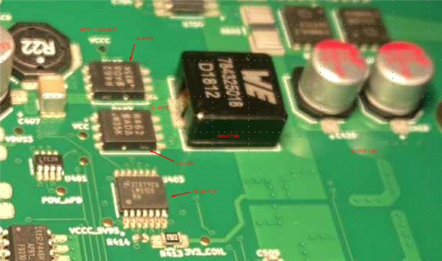
I'm using the LM3150 with 20V input to supply a 3.3V rail. These are my schematics:

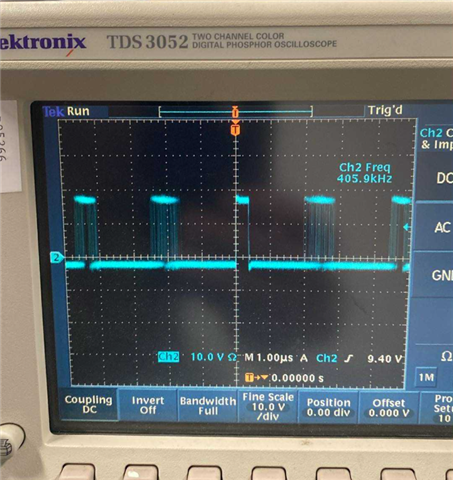
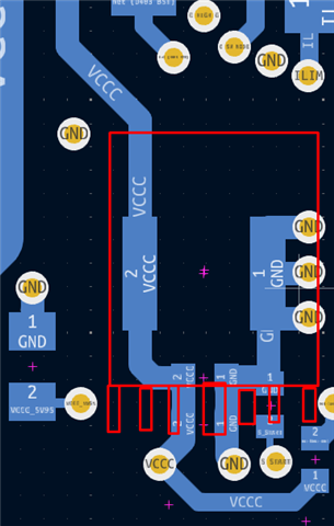
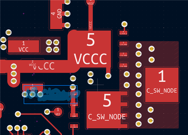
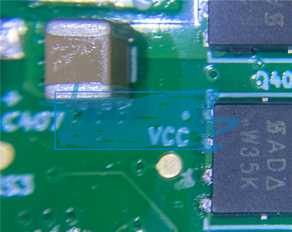
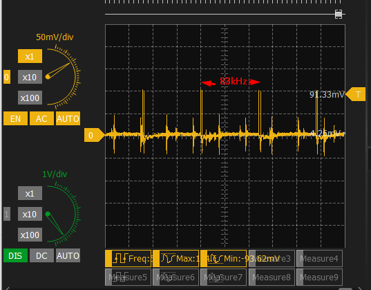
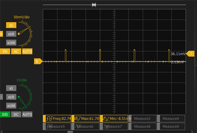
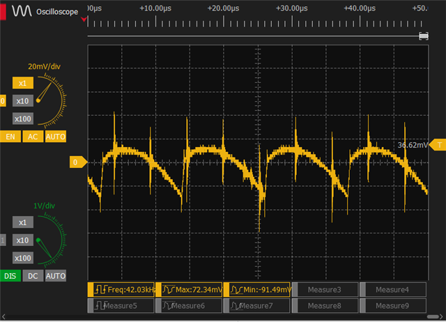
VCC, VCCC, I can measure and are at 20V.
VCC5V95V I can measure and is at 5.95V.
C406, C407, C413, C414, C415, and C416 are all 50V rating.
C405 has a 35V rating.
C421 and C422 are 10V rating.
S_START and other nets with labels are not routed elsewhere on the board.
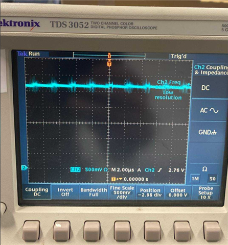
What does this mean?
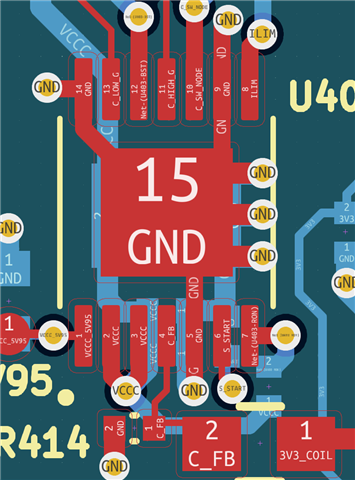
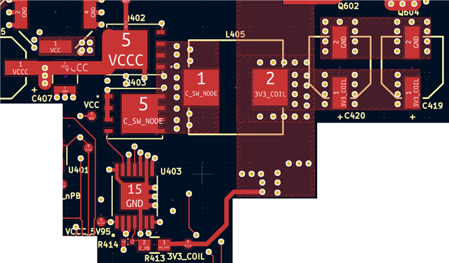
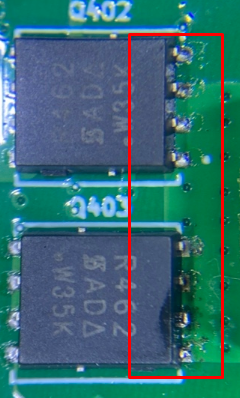
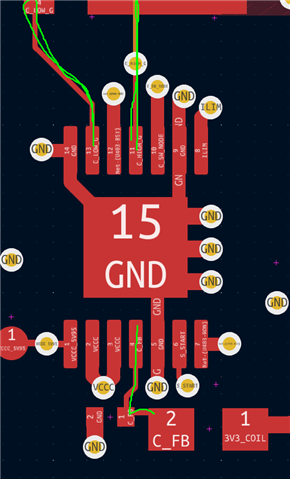
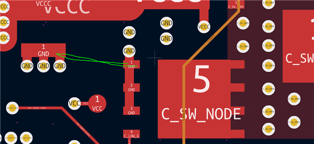
This is my layout on the top: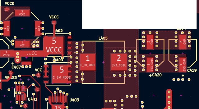
This is my layout on the bottom:
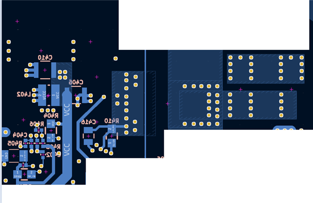
The layout is tough to see from pictures, but basically I have kept my switch node as small as possible very very similar to the reference layout. The only difference from the reference layout is that I wasn't able to route the C_HIGH_G and C_LOW_G nets through the NMOS as they did in the reference design.
What have I done incorrectly?