HD3SS3220: Schematic Review

Part Number: HD3SS3220
Other Parts Discussed in Thread: 3220DFP-DGLEVM, TPS25910, TUSB211A, TUSB211, CSD17313Q2, TPD1E05U06

Tool/software:

Dear Specialists,

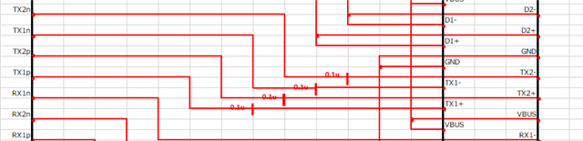
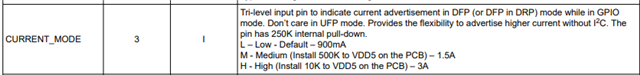
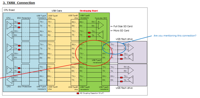
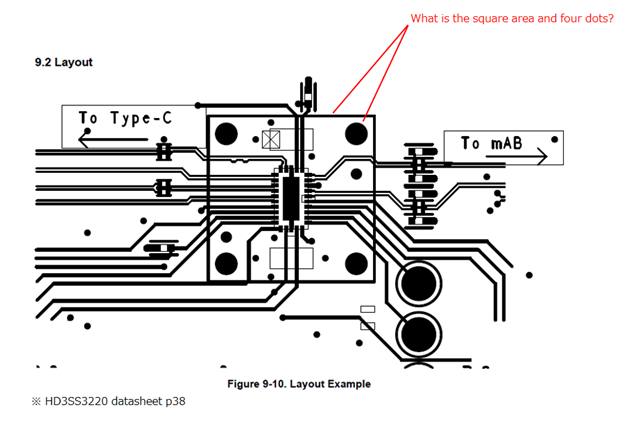
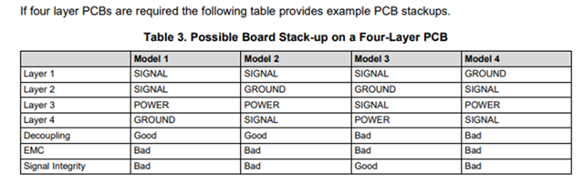
My customer is considering HD3SS3220 and has a request of schematic review.

Could you please review the attached Excel file and provide your advice.

If you need an additional information, could you please let me know.

I appreciate your great help in advance.

Best regards,

Shinichi

  • Hi Shinichi,

    I am trying to open the excel file you sent, however I am receiving an error. I will send you an E2E friend request, could you accept that and send the schematic to me directly? I can review the schematic from there.

    Thanks,

    Ryan

  • Hi Shinichi,

    Are you intending to route the HD3SS3220 as a DFP, UFP, or DRP? It looks like a DFP might be intended, however it is currently configured as a DRP. The port pin should be pulled-up for a DFP configuration.

    For a DFP connection, the ID pin needs to be pulled up to VDD with a 200KOhm resistor. Additionally, the ID pin needs to be used to control VBUS through a VBUS switch. VBUS being sent through the type-C connector is part of the CC negotiation process, and should only be sent when ID is pulled low. I would recommend adding a power switch that is enabled when the EN pin pulled low, and attached to the ID pin.

    Are you intending this for a passthrough application, I.E The signal coming in from the type-B port goes out the TX of the type-C port, and vice-versa? Or will the board you are developing have a controller interfacing with the TX/RX of these ports?

    If you intend to use the HD3SS3220 as a pass-through, then the RX of the type-B port should connect to the TXp/n of the HD3SS3220, and the TX of the type-B port should connect to the RXP/N of the HD3SS3220. That way, the signal coming in from the type-B port from the RX pins is routed to the TX of the type-C connector, and vice-versa.

    If acting as a passthrough, these caps on the TX lanes should not be needed, as the TX signal should already be coupled at the host/CPU.

    For a DFP application, the VBUS_DET pin can be left floating, it is not required.

    The CURRENT_MODE pin should be either pulled-up or pulled-down, according to the amount of current you want to advertise:

    Correctly, if the polarities of the lanes are swapped there should be no issue. Compliant USB3 Phy's should support polarity inversion.

    Please let me know if you have any other questions.

    Thanks,

    Ryan

  • Hi Ryan,

    Thank you for your reply.

    I'll share these information with the customer.

    When the customer has an additional question, I consult you again.

    I appreciate your great help and cooperation.

    Best regards,

    Shinichi

  • Hi Shinichi,

    Sounds good. Let me know if any other questions come up.

    Thanks,

    Ryan

  • HI Ryan,

    Thank you for your reply.

    The customer has additional questions.

    Could you please advise?

    ---

    Our developing board, there is not controller.

    VBUS comes from CPU board with USB3.0 Type-B connector and passthrough the USB3.0 Type-C  output.

    For a DFP connection, the ID pin needs to be pulled up to VDD with a 200KOhm resistor. Additionally, the ID pin needs to be used to control VBUS through a VBUS switch. VBUS being sent through the type-C connector is part of the CC negotiation process, and should only be sent when ID is pulled low. I would recommend adding a power switch that is enabled when the EN pin pulled low, and attached to the ID pin.

    → p28 is indeed pulled up to VBUS with 200kΩ.
    Our board does not have a control circuit, and ID pin is output .
    Since there is nothing to connect to, it is unclear why it is pulled up to VBUS with 200kΩ.

    Even in this case, is it necessary to pull it up with 200kΩ?
    Is it to prevent the terminal from becoming unstable when set to Hi-Z because it is an open-drain output terminal?

    If you intend to use the HD3SS3220 as a pass-through, then the RX of the type-B port should connect to the TXp/n of the HD3SS3220, and the TX of the type-B port should connect to the RXP/N of the HD3SS3220. That way, the signal coming in from the type-B port from the RX pins is routed to the TX of the type-C connector, and vice-versa.

    I thought that Type B TX+ would connect to Type C TX1+ and TX2+, and that the HD3SS3220 would just switch between TX1+ and TX2.

     Is it correct to connect Type B TX+ to Type C RX1+ and RX2+?

    Could you please explain for more detail.

    For a DFP application, the VBUS_DET pin can be left floating, it is not required.

    Just to confirm, does this comment applies to DFP pass-through mode.

    The CURRENT_MODE pin should be either pulled-up or pulled-down, according to the amount of current you want to advertise:

    If using at 900mA, is floating fine?

    The customer revised the schematic.

    Could you please confirm and advise?

    Question about HD3SS3220 20250814 .xlsx

    I appreciate your great help and cooperation.

    Best regards,

    Shinichi

  • Hi Shinichi,

    → p28 is indeed pulled up to VBUS with 200kΩ.
    Our board does not have a control circuit, and ID pin is output .
    Since there is nothing to connect to, it is unclear why it is pulled up to VBUS with 200kΩ.

    Even in this case, is it necessary to pull it up with 200kΩ?
    Is it to prevent the terminal from becoming unstable when set to Hi-Z because it is an open-drain output terminal?

    On the revised schematic, it still looks like the ID pin is floating. This pin is an open-drain, so it needs to be connected to something like VDD5 or VCC3 with a 200Kohm resistor. Additionally, there needs to be a power switch on the board which is controlling VBUS.

    The ID pin is used to control when VBUS is sent to the type-C connector, in this case from the type-B port. This can be done by implementing a power switch, and routing the ID pin to the EN pin of that power switch. Then, once there is a connection, the ID pin will be pulled low, which should indicate for the switch to enable sending VBUS to the type- Connector.

    If ID is not used to control when VBUS goes to the type-C connector, then that will cause issues with the CC negotiation, resulting in either only one side working, or no USB3 connection working. I would recommend looking at our 3220DFP-DGLEVM for an example of what this application should look like. 

    I thought that Type B TX+ would connect to Type C TX1+ and TX2+, and that the HD3SS3220 would just switch between TX1+ and TX2.

     Is it correct to connect Type B TX+ to Type C RX1+ and RX2+?

    Could you please explain for more detail.

    The Type B TX+/- is actively send a signal OUT of the type-B connector, and the same goes for the TX1/2 +/- pins of the type-C connector, where these pins are actively sending a signal OUT of the type-C connector. If you route these two lines together, there will be no signals moving through the device.

    As such, you should route the RX of the type-B connector, which receives signal from the type-B cable, to the TX of the type-C connector, which will transmit this signal through the type-C cable. And you should route the RX of the type-C connector to the TX of the type-B connector.

    In this case, SSTX of the HD3SS3220 would route to the RX of the type-B connector, while the SSRX of the HD3SS3220 would route to the TX of the type-B connector. Then, you would route the TX1/2 pins of the HD3SS3220 to the TX pins of the type-C connector, and the RX1/2 pins to the RX pins of the type-C connector.

    That way, the signal received by the type-B port is transmitted out the type-C port, and the signal received by the type-C port is transmitted out the type-B port. You want this board to essentially act as a passthrough for these signals.

    For a DFP application, the VBUS_DET pin can be left floating, it is not required.

    Just to confirm, does this comment applies to DFP pass-through mode.

    Correct, this pin is not needed for any DFP application.

    The CURRENT_MODE pin should be either pulled-up or pulled-down, according to the amount of current you want to advertise:

    If using at 900mA, is floating fine?

    This should be okay as well, yes.

    The customer revised the schematic.

    Could you please confirm and advise?

    Please ensure the TX/RX lanes are correctly routed.

    Caps look fine, if its acting as a passthrough then caps shouldn't be a concern unless caps are missing on the host board.

    I'm assuming I2C isn't being used, so SDA/SCL and ADDR being floating works as well.

    I don't have any other notes aside from what is listed above. Please make sure ID is being used correctly with a power switch, and that the TX/RX lanes are correctly routed.

    Thanks,

    Ryan

  • Hi Ryan,

    Thank you for your reply.

    I shared your suggestion with the customer.

    The customer has additional question.

    Could you please see below and advise?

    Also revised schematic is ver.3 of the attached file.

    ---

    1. Can the attached schematic achieve DFP pass-through between a Type-B receptacle and a Type-C receptacle?

    2. In the attached schematic, the HD3SS3220 acts as a DFP, and will the HD3SS3220's CC pin be pulled up with 56kΩ?
    (DFP Default USB Power)

    3.

    As such, you should route the RX of the type-B connector, which receives signal from the type-B cable, to the TX of the type-C connector, which will transmit this signal through the type-C cable. And you should route the RX of the type-C connector to the TX of the type-B connector.

    In our case, a Type-C USB memory stick is connected to the Type-C receptacle, not a Type-C cable.
    Please refer to the system configuration diagram at the top of the updated document.
    Would the answer be the same in this case?
    Please let me know if there are any difference in the answers.

    ④In your answer, you said:

    In this case, SSTX of the HD3SS3220 would route to the RX of the type-B connector, while the SSRX of the HD3SS3220 would route to the TX of the type-B connector. Then, you would route the TX1/2 pins of the HD3SS3220 to the TX pins of the type-C connector, and the RX1/2 pins to the RX pins of the type-C connector.

    This connects the TX of the Type-B to the RX of the Type-C (cross connection).

    However, for the 3220DFP-DGLEVM,
    Wire the SSTX of the HD3SS3220 to the RX of the Type-A connector, and wire the SSRX of the HD3SS3220 to the TX of the Type-A connector.
    Next, wire the TX1/2 pins of the HD3SS3220 to the RX pin of the Type-C connector, and the RX1/2 pins of the HD3SS3220 to the TX pin of the Type-C connector

    .For the 3220DFP-DGLEVM, the Type A TX connects to the Type C TX (straight connection). This differs from your answer (cross connection).
    Is the reason for this difference because, in my case, I have a cross cable with a Type A plug and a Type B plug between the board on which the HD3SS3220 is installed and the CPU board? (Please refer to the attached system configuration diagram at the top.)
    Please explain the reason.

    ⑤ Regarding the D± connection,
    The 3220DFP-DGLEVM uses a TUSB211RWB.

    Our schematic directly connects the D± of the Type B receptacle and the Type C receptacle. Is this okay?

    Question about HD3SS3220 20250814.xlsx

    ---

    I appreciate your great help and cooperation.

    Best regards,

    Shinichi

  • Hi Shinichi,

    1. Can the attached schematic achieve DFP pass-through between a Type-B receptacle and a Type-C receptacle?

    Please ensure the VBUS being supplied to the type-C controller is the VBUS being output by the TPS25910. Otherwise, it looks like it should be setup correctly, yes.

    2. In the attached schematic, the HD3SS3220 acts as a DFP, and will the HD3SS3220's CC pin be pulled up with 56kΩ?
    (DFP Default USB Power)

    There should be no need to externally pull-up the CC pins. CC controllers on both sides of the type-C connection should be able to handle the pull-up and pull-downs on the CC lanes as needed.

    In our case, a Type-C USB memory stick is connected to the Type-C receptacle, not a Type-C cable.
    Please refer to the system configuration diagram at the top of the updated document.
    Would the answer be the same in this case?
    Please let me know if there are any difference in the answers.

    Yes, it would still be the same in terms of routing. The TX of the connector will connect to the RX of the memory stick, and vice-versa.

    This connects the TX of the Type-B to the RX of the Type-C (cross connection).

    However, for the 3220DFP-DGLEVM,
    Wire the SSTX of the HD3SS3220 to the RX of the Type-A connector, and wire the SSRX of the HD3SS3220 to the TX of the Type-A connector.
    Next, wire the TX1/2 pins of the HD3SS3220 to the RX pin of the Type-C connector, and the RX1/2 pins of the HD3SS3220 to the TX pin of the Type-C connector

    .For the 3220DFP-DGLEVM, the Type A TX connects to the Type C TX (straight connection). This differs from your answer (cross connection).
    Is the reason for this difference because, in my case, I have a cross cable with a Type A plug and a Type B plug between the board on which the HD3SS3220 is installed and the CPU board? (Please refer to the attached system configuration diagram at the top.)
    Please explain the reason.

    This is primarily because of the type-A plug that's on this EVM, as opposed to the type-B receptacle you are using on this board. In this case, the UFP EVM would be most similar to how you should route the TX and RX signals through the HD3SS3220. Right now in the schematic though, it looks like you have it configured correctly.

    ⑤ Regarding the D± connection,
    The 3220DFP-DGLEVM uses a TUSB211RWB.

    Our schematic directly connects the D± of the Type B receptacle and the Type C receptacle. Is this okay?

    I would recommend using the TUSB211A over the TUSB211 in this case, just because it's newer, and has AC and DC boost while the TUSB211 only has AC boost. Yes, you can just directly route D+ to D+ from connector to connector, these lanes are bidirectional. Make sure the TUSB211A is set to a lower setting at the start to avoid over-compensation.

    Thanks,

    Ryan

  • Hi Ryan,

    Thank you for your reply.

    The customer's understanding of the HD3SS3220 is improving.

    The customer has revised the connection diagram based on your advice.
    Please check version 4 of the attached Excel file.

    Also the customer has additional questions.

    Could you please advise?

    ーーー

    Please ensure the VBUS being supplied to the type-C controller is the VBUS being output by the TPS25910. Otherwise, it looks like it should be setup correctly, yes.

    In the previous circuit, the Type B receptacle's VBUS, the Type C receptacle's VBUS, and the HD3SS322's VBUS were all common.
    I separated the VBUS based on the reference circuit (pp. 7, 8) of the "HD3SS3220 DFP Dongle Evaluation Module."
    I have updated the attached "Connection diagram using HD3SS3220 and TLV77033_250903.xlsx" and separated it into VBUS_A (green) and VBUS_C (blue).
    Just to be safe, I have also color-coded VCC33 (orange).
    Is there a problem with this connection?

    There should be no need to externally pull-up the CC pins. CC controllers on both sides of the type-C connection should be able to handle the pull-up and pull-downs on the CC lanes as needed.

    We have set it as a fixed DFP.
    At this point, the 3220 should be in a 56kΩ pull-up state. Is this understanding correct?

    We want to ensure that the HD3SS3220 is the DFP even when a smartphone is connected to our device.
    This is to prevent VBUS conflicts.

    Yes, it would still be the same in terms of routing. The TX of the connector will connect to the RX of the memory stick, and vice-versa.

    Where in the attached circuit diagram do the TX of the connector and RX of the memory stick you mentioned refer to?
    (I would understand if you were referring to the TX of the memory stick connector and the RX of the memory stick receiving IC)

    I would recommend using the TUSB211A over the TUSB211 in this case, just because it's newer, and has AC and DC boost while the TUSB211 only has AC boost. Yes, you can just directly route D+ to D+ from connector to connector, these lanes are bidirectional. Make sure the TUSB211A is set to a lower setting at the start to avoid over-compensation.

    Therefore, I don't think a signal conditioner like the TUSB211A is necessary.
    Is there anything we should change in our connection diagram?

    Question about HD3SS3220 20250904.xlsx

    ---

    I appreciate your great help and cooperation.

    Best regards,

    Shinichi

  • Hi Shinichi,

    In the previous circuit, the Type B receptacle's VBUS, the Type C receptacle's VBUS, and the HD3SS322's VBUS were all common.
    I separated the VBUS based on the reference circuit (pp. 7, 8) of the "HD3SS3220 DFP Dongle Evaluation Module."
    I have updated the attached "Connection diagram using HD3SS3220 and TLV77033_250903.xlsx" and separated it into VBUS_A (green) and VBUS_C (blue).
    Just to be safe, I have also color-coded VCC33 (orange).
    Is there a problem with this connection?

    Looks better to me, I don't have any issues with this. I would just say make sure the TPS device is configured correctly per the current needed for your connection.

    We have set it as a fixed DFP.
    At this point, the 3220 should be in a 56kΩ pull-up state. Is this understanding correct?

    We want to ensure that the HD3SS3220 is the DFP even when a smartphone is connected to our device.
    This is to prevent VBUS conflicts.

    Makes sense. I just wanted to make sure there was no external pull-up, as the HD3SS3220 should be able to handle this by itself.

    As long as the HD3SS3220 is set as a DFP via the PORT pin, as it currently is, then it should only configure as a DFP. This means the port will only function with a UFP or DRP role device.

    Where in the attached circuit diagram do the TX of the connector and RX of the memory stick you mentioned refer to?
    (I would understand if you were referring to the TX of the memory stick connector and the RX of the memory stick receiving IC)

    I'm referring to the type-C connector on your board. The TX pins of the Type-C connector will connect to the RX pin's of the USB-C flash drive that connects to that port.

    Therefore, I don't think a signal conditioner like the TUSB211A is necessary.
    Is there anything we should change in our connection diagram?

    This depends on the system length. What is the expected length of the USB cable you are using between the CPU board and the developing board? If it's a decent length, it may be worth implement a USB3 and USB2 redriver.

    Thanks,

    Ryan

  • Hi Ryan,

    Thank you for your reply.

    The customer has additional question.

    Could you please advise?

    ---

    Looks better to me, I don't have any issues with this. I would just say make sure the TPS device is configured correctly per the current needed for your connection.

    VBUS should be used at 0mA to 900mA.
    According to formula (2) on page 7 of the TPS25910 datasheet, when ILIM = 0.9A, RLIM = 218.787876kΩ.
    From page 9 of the TPS25910 datasheet, I understand that a 1% resistor is required.
    Therefore, a 220kΩ 1% resistor is used for RLIM. The attached document has been revised.
    Could you please confirm that this value is acceptable.

    Makes sense. I just wanted to make sure there was no external pull-up, as the HD3SS3220 should be able to handle this by itself.

    As long as the HD3SS3220 is set as a DFP via the PORT pin, as it currently is, then it should only configure as a DFP. This means the port will only function with a UFP or DRP role device.

    Just to be sure,
    When the HD3SS3220 is configured as a DFP, is the CC pin internally pulled up with 56kΩ within the HD3SS3220?

    I'm referring to the type-C connector on your board. The TX pins of the Type-C connector will connect to the RX pin's of the USB-C flash drive that connects to that port.

    The attached document has been updated. "3. TXRX Connection Diagram" has been added to the right of "1. System Configuration Diagram."
    Are you referring to the blue circle in "3. TXRX Connection Diagram"?

    Could you please see attached file for more detail.

    Question about HD3SS3220 20250905.xlsx

    This depends on the system length. What is the expected length of the USB cable you are using between the CPU board and the developing board? If it's a decent length, it may be worth implement a USB3 and USB2 redriver.

    In our case, the transmission length for USB 3.2 Gen 1 is approximately 1m.
    Therefore, we think that a redriver is not necessary.

    ---

    I appreciate your great help and cooperation.

    Best regards,

    Shinichi

  • Hi Shinichi,

    VBUS should be used at 0mA to 900mA.
    According to formula (2) on page 7 of the TPS25910 datasheet, when ILIM = 0.9A, RLIM = 218.787876kΩ.
    From page 9 of the TPS25910 datasheet, I understand that a 1% resistor is required.
    Therefore, a 220kΩ 1% resistor is used for RLIM. The attached document has been revised.
    Could you please confirm that this value is acceptable.

    Sounds good to me. If you don't intend on using any higher current, that should be okay.

    Just to be sure,
    When the HD3SS3220 is configured as a DFP, is the CC pin internally pulled up with 56kΩ within the HD3SS3220?

    Yes, the HD3SS3220 will provided the pull-up resistance needed for default operation internally.

    I'm referring to the type-C connector on your board. The TX pins of the Type-C connector will connect to the RX pin's of the USB-C flash drive that connects to that port.

    The attached document has been updated. "3. TXRX Connection Diagram" has been added to the right of "1. System Configuration Diagram."
    Are you referring to the blue circle in "3. TXRX Connection Diagram"?

    Yes, this is the connection I was referring to. Looks fine to me here, I don't have any issues.

    In our case, the transmission length for USB 3.2 Gen 1 is approximately 1m.
    Therefore, we think that a redriver is not necessary.

    My only concern, with the amount of connectors and cable lengths mix with the inherent loss from the mux in the HD3SS3220, is that the loss for a 10Gbps signal will still be high. If possible, an estimation of the amount of loss in the system would be better, just to ensure it is not exceeding the loss budget.

    Thanks,

    Ryan

  • Hi Ryan,

    Thank you for your reply.

    Could you please advise the additional questions?

    ---

    (1)

    In our case, the transmission length for USB 3.2 Gen 1 is approximately 1m.
    Therefore, we think that a redriver is not necessary.

    My only concern, with the amount of connectors and cable lengths mix with the inherent loss from the mux in the HD3SS3220, is that the loss for a 10Gbps signal will still be high. If possible, an estimation of the amount of loss in the system would be better, just to ensure it is not exceeding the loss budget.

    We plans to use USB3.2 Gen 1 whose speed is 5Gbps, not 10Gbps.

    In this case, transmission length is less than 2m, it should be no problem.

    Are there any concern?

    (2) Chapter 9.1.1 of the HD3SS3220 datasheet states that six layers are recommended.

    Could you please let me know why six layers are recommended?

    Also, due to cost constraints, anything other than four layers is unlikely to be adopted. 

    Is it possible to achieve it with four layers?

    (3) I understand that the the datasheet 9.1.7 of page 37 and Figure 9-8 of the HD3SS3220 datasheet describe AC ​​coupling capacitors.

    In this section, it is recommended partially voiding the SMD mounting pads of the reference plane by approximately 60% because this value strikes a balance between the capacitive effects of a 0% reference void and the inductive effects of a 100% reference void

    Is this the correct location for 60% cavity formation?

    Could you please see attached Voiding of excel file?

    (4) Regarding Figure 9-10. 

    What do the square area and four dots represent?

    Could you please see Layout  of excel file?

    Question about capacitor and board layout.xlsx

    ---

    I appreciate your great help and cooperation.

    Best regards,

    Shinichi

  • Hi Shinichi,

    We plans to use USB3.2 Gen 1 whose speed is 5Gbps, not 10Gbps.

    In this case, transmission length is less than 2m, it should be no problem.

    Are there any concern?

    The need for a redriver is typically more based on the loss of a system, rather than the length. In this case, with so many cables and connectors, it's possible there is a higher than average loss. I would recommend the customer determining the loss attributed to their cables and connectors, as well as their layout, and finding out how much loss is in their system.

    (2) Chapter 9.1.1 of the HD3SS3220 datasheet states that six layers are recommended.

    Could you please let me know why six layers are recommended?

    Also, due to cost constraints, anything other than four layers is unlikely to be adopted. 

    Is it possible to achieve it with four layers?

    We recommend this to avoid having the VCC layer right next to a data path layer, such as the top or bottom layer, as VCC can cause noise in data signaling if the data signaling is not properly isolated.

    (3) I understand that the the datasheet 9.1.7 of page 37 and Figure 9-8 of the HD3SS3220 datasheet describe AC ​​coupling capacitors.

    In this section, it is recommended partially voiding the SMD mounting pads of the reference plane by approximately 60% because this value strikes a balance between the capacitive effects of a 0% reference void and the inductive effects of a 100% reference void

    Is this the correct location for 60% cavity formation?

    Could you please see attached Voiding of excel file?

    I would recommend the customer looks at our high-speed layout design guidelines app note, this has more information on this: https://www.ti.com/lit/an/slla414/slla414.pdf?ts=1757368993497&ref_url=https%253A%252F%252Fwww.ti.com%252Fproduct%252FHD3SS3220

    (4) Regarding Figure 9-10. 

    What do the square area and four dots represent?

    Could you please see Layout  of excel file?

    These were used in our EVM to allow for a socket to be used to freely place and remove HD3SS3220 units for testing. These can be ignored for a solder-down layout.

    Thanks,

    Ryan

  • Hi Ryan,

    Thank you for your reply.

    (1)

    The need for a redriver is typically more based on the loss of a system, rather than the length. In this case, with so many cables and connectors, it's possible there is a higher than average loss. I would recommend the customer determining the loss attributed to their cables and connectors, as well as their layout, and finding out how much loss is in their system.

    The customer estimated the total insertion loss.

    The customer's system configuration is:
    a [CPU board (Type A female) (50mm wiring length)] (estimated loss 2dB) ⇔ b [1m cable (Type A male, Type B male)] (estimated loss 2.5dB) ⇔ c [Development board (Type B female, Type C female) (board size 85mm)] (estimated loss 3.3dB (85mm winding) + 1.04dB (HD3SS3220)) ⇔ d [USB memory (Type C male)] (2.5dB)

    Therefore, the total insertion loss is (2 + 2.5 + 4.34 + 2.5) = 11.34dB << 20dB.

    The customer does not think a re-driver is necessary.

    (2) Regarding Section 9.1.4 High-Speed ​​Differential Signaling Rules

    If the differential pair rules in Section 9.1.4 are followed, can the five components (HD3SS3220, TLV77033, TPS25910, CSD17313Q2, and TPD1E05U06) be placed on the TOP or BOTTOM layer? 

    For example, 

    Can an LDO be placed on the backside of a high-speed differential line?

    Can an LDO be placed if it's 50 mil away from the differential pair?

    (3) 

    We recommend this to avoid having the VCC layer right next to a data path layer, such as the top or bottom layer, as VCC can cause noise in data signaling if the data signaling is not properly isolated.

    You mentioned that power layers should not be adjacent to the top or bottom layers, but looking at Layer 6 in Table 9.1, the power layer is L5, which is adjacent to the bottom layer.

    Also, can I assume that the data path you mentioned refer to differential pairs?

    If so, there is a rule in Section 9.1.4 that requires GND to be placed on adjacent layers, and I would follow that rule.

    Is there anything else you intended?

    By the way, the document you introduced mentioned a four-layer board. I think four layer board is possible, though difficult.

    Is this understanding correct?

    In the datasheet and application note(High-Speed Layout Guidelines for Signal Conditioners and USB Hubs), I couldn't understand the reason why 6 layer board is recommended.

    I think that a four-layer board should be fine as long as 9.1.4 High-Speed ​​Differential Signal Rules are observed.

    Could you please advise?

    (4) In Figure 9-1 of the HD3SS3220 datasheet, should the serpentine wiring be placed on the IC side or the connector side?

    Or should I place it on the mismatched end as specified in the datasheet?

    (5) 

    I would recommend the customer looks at our high-speed layout design guidelines app note, this has more information on this: https://www.ti.com/lit/an/slla414/slla414.pdf?ts=1757368993497&ref_url=https%253A%252F%252Fwww.ti.com%252Fproduct%252FHD3SS3220

    I looked at the document you specified. The information on page 22 of application note differs from the information on page 37 of the HD3SS3220 datasheet.

    The cavity has changed from 60% to 100%.
    The capacitor size has changed from 0402 to 0201.
    Which information should I use?

    If datasheet(60%) is correct, could you please let me know if the following understanding is correct.

    Question about capacitor layout.xlsx

    (6) The customer would like to obtain the layout sample of HD3SS3220 application circuit.

    Could you provide the layout of 3220DFP-DGLEVM.

    Also, could you please provide any other reference materials.

    ---

    I appreciate your great help and cooperation.

    Best regards,

    Shinichi

  • Hi Shinichi,

    Therefore, the total insertion loss is (2 + 2.5 + 4.34 + 2.5) = 11.34dB << 20dB.

    The customer does not think a re-driver is necessary.

    My only concern would be if a customer used a cable to extend the port to connect their flash drive, but otherwise yes the amount of loss is still within the allowed budget, a redriver is not required.

    If the differential pair rules in Section 9.1.4 are followed, can the five components (HD3SS3220, TLV77033, TPS25910, CSD17313Q2, and TPD1E05U06) be placed on the TOP or BOTTOM layer? 

    I believe these units can be placed on the top or bottom layer, yes. I would ensure that the SS differential signaling is isolated from any power devices/lines/planes.

    You mentioned that power layers should not be adjacent to the top or bottom layers, but looking at Layer 6 in Table 9.1, the power layer is L5, which is adjacent to the bottom layer.

    Also, can I assume that the data path you mentioned refer to differential pairs?

    If so, there is a rule in Section 9.1.4 that requires GND to be placed on adjacent layers, and I would follow that rule.

    Is there anything else you intended?

    You can have a power layer adjacent to a signal layer, however the power layer would need to be designed such that there are no power planes directly next to any SS differential pairs, it would also be best to use GND vias to isolate the SS signaling.

    My best recommendation would be to have a GND layer adjacent to signaling layers.

    In the datasheet and application note(High-Speed Layout Guidelines for Signal Conditioners and USB Hubs), I couldn't understand the reason why 6 layer board is recommended.

    I think that a four-layer board should be fine as long as 9.1.4 High-Speed ​​Differential Signal Rules are observed.

    Could you please advise?

    While it's possible, I'm not sure I would recommend it. As you can see in this table, it's also mentioned that certain aspects of the signal will suffer, such as EMC performance and signal integrity. It's safer to follow the PCB stackups suggested in 9.1.1 of the HD3SS3220 datasheet.

    The cavity has changed from 60% to 100%.
    The capacitor size has changed from 0402 to 0201.
    Which information should I use?

    We recommend 0201 size capacitors for AC coupling, and a 100% void.

    (6) The customer would like to obtain the layout sample of HD3SS3220 application circuit.

    Could you provide the layout of 3220DFP-DGLEVM.

    Also, could you please provide any other reference materials.

    Please accept my E2E friend request, which I believe I sent previously, and I can send those files over.

    Thanks,

    Ryan

  • Hi Ryan,

    Thank you for your reply.

    Could you please advise additional questions listed below?

    ---

    (1)

    You can have a power layer adjacent to a signal layer, however the power layer would need to be designed such that there are no power planes directly next to any SS differential pairs, it would also be best to use GND vias to isolate the SS signaling.

    My best recommendation would be to have a GND layer adjacent to signaling layers.

    In our case, the only power device is the TLV77033PDBVR.

    According to 9.1.3 Differential Signal Spacing,

    ・Is it okay to keep the TLV77033PDBVR 50 mils away from the differential pair?

    ・The only power lines/planes are VBUS_A, VBUS_C, and VCC33. Is it okay to keep these 50 mils away from the differential pair?

    ・Also, can I place the TLV77033PDBVR on the backside of the differential pair?

    (2) According to 9.1.2 High-Speed Signal Trace Length Matching,

    It says to place serpentine routing in the "Length-Matching at Mismatched Ends" section.

    ・Should the serpentine routing be placed on the IC side or the connector side?

    ・Or are there any specifications for the location of the serpentine routing?

    ーーー

    I appreciate your great help and cooperation.

    Best regards,

    Shinichi

  • Hi Shinichi,

    According to 9.1.3 Differential Signal Spacing,

    ・Is it okay to keep the TLV77033PDBVR 50 mils away from the differential pair?

    ・The only power lines/planes are VBUS_A, VBUS_C, and VCC33. Is it okay to keep these 50 mils away from the differential pair?

    ・Also, can I place the TLV77033PDBVR on the backside of the differential pair?

    We recommend the distance be 5 times the width of the differential routing used for the pair. So whatever the distance is between TXp and TXn, five times that would be the best minimal distance from the differential pair.

    Placing the TLV on the opposite side of the board should be okay, so long as there is a ground layer between the differential pair and the TLV.

    (2) According to 9.1.2 High-Speed Signal Trace Length Matching,

    It says to place serpentine routing in the "Length-Matching at Mismatched Ends" section.

    ・Should the serpentine routing be placed on the IC side or the connector side?

    ・Or are there any specifications for the location of the serpentine routing?

    We recommend the serpentine routing be done closer to where this intra-pair skew is occurring. So if it's occurring closer to the connector, it would be better closer to the connector, the IC, vice-versa.

    Thanks,

    Ryan