Other Parts Discussed in Thread: UCC5390
Tool/software:
Hello,
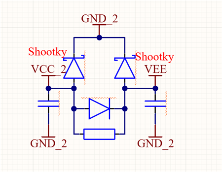
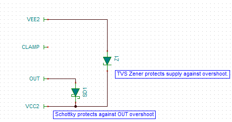
While reviewing reference designs for the UCC5390-Q1 isolated gate driver, I found a circuit similar to the attached schematic. In this design, Schottky diodes are placed between VCC2, VEE, and GND2 nodes. I would like to confirm whether this configuration is suitable as a protection network (e.g., against negative transients, false turn-on, gate return currents, etc.).
Could you please clarify:
-
Is this topology appropriate for protecting the secondary side of the UCC5390-Q1? In which scenarios is it recommended or not recommended?
-
Are the diode placements and current directions correct? Would you suggest a TVS diode or another protection approach instead?
-
For diode selection (e.g., B240A-13-F), what criteria should be used regarding reverse voltage, current rating, leakage, and recovery?
-
Does this network affect power-up/power-down sequencing or negative VGS limits (benefits or risks)?
-
Is this configuration explicitly recommended in the datasheet or application notes? If so, could you point me to the relevant section/figure?
Thank you in advance for your support.