TPS7A57: How to connect a TPS7A57 as a constant current source

Part Number: TPS7A57

Tool/software:

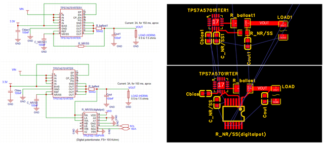
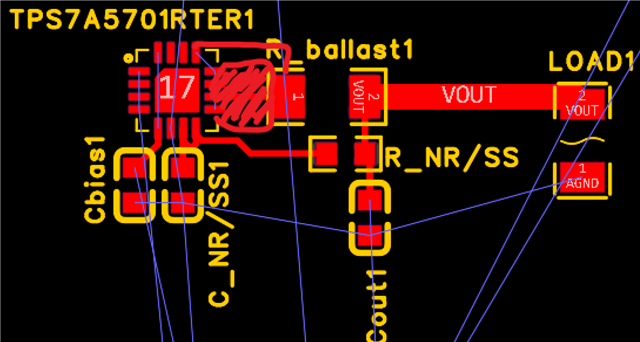
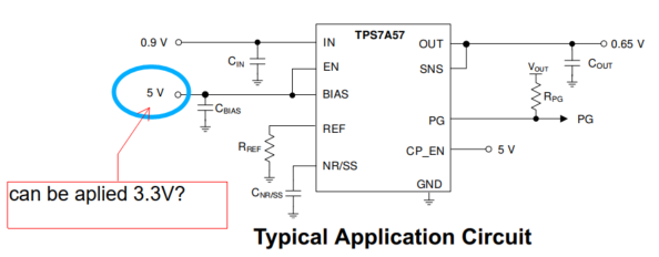
Hello, good afternoon. How to connect a TPS7A57 as a current source for a very specific application. My load has low resistance (between 0.5 ohms and 1.5 ohms) and I want to apply a direct current of 3 amps to it. If I do the math, the output voltage will be between (V=R*I) 1.5 volts and 4.5 volts, so I understand the regulator's input voltage will be those values ​​plus the dropout value of 75mV, or 1.575V to 4.575V. My idea is to regulate the input voltage so that heat dissipation in the regulator is minimal. My question then is how to convert this voltage regulator to a constant current source. I need this current to be present for only approximately 150 ms and then turn off, which I plan to do by controlling the Enable pin. Thank you very much.

  • Hi Gabriel,

    I show how to do this for a single or any number in parallel in this document.  See slide 27 in the first presentation.  In essence you need to rotate the NR/SS resistor to connect to Vload, and place a small series resistor between OUT and Vload.  The voltage induced across the two resistors must match.  You use this technique regardless of whether a single LDO is used or multiple LDOs are used in parallel. See the collateral and let us know if you have any questions.

    https://www.ti.com/lit/ml/slup424/slup424.pdf?ts=1755877321878

    https://www.ti.com/lit/ml/slup415/slup415.pdf?ts=1755877333348

    Thanks,

    Stephen

  • Hi Stephen.First, thank you very much for your prompt response. I have another question: what is the lowest ballast resistance value? I want it to be the lowest possible value since in my application the dissipated power (if I use a value of RB = 50 milliohms as mentioned in the application note) is equal to P = R * I ^ 2 = 0.05 * 3 * 3 = 0.45 watts, which means I have to use a somewhat large resistor size for my design, which has limited space on my PCB. If I could use a smaller RB value, I could reduce the resistor size.
    The second question is your opinion on whether the design I'm considering would work, considering the low resistance value of my load, the current I want to use, and the power that the TPS7A57 regulator can dissipate. Thank you very much!

  • Hi Gabriel,

    What you are exploring involves pulsed loading and from a thermal perspective you should be reviewing the transient thermal impedance of your design.  This is not published in modern LDO datasheets that I'm aware of, but you are in luck - we are just starting to add this to our datasheets for our performance LDO's including this one.  The JEDEC PCB standard is usually pessimistic while an EVM may be more realistic (but if your PCB is very dense with components, the EVM may be optimistic).  We have simulation data on these values and we are in the process of updating the datasheet. At 200ms the simulations show JEDEC = 13 C/W and EVM = 10 C/W.  What you can dissipate will depend on your ambient temperature and what you set Vin to.  If you maintain 400mV from Vin - Vout (as per the datasheet typical graphs) and you drive 3A into the load, you will see 1.2W dissipation across the LDO.  This will cause the junction to rise 12-16C above ambient.  You can lower Vin to give 300mV of headroom to achieve slightly worse performance but less temperature rise (but look at the datasheet to confirm this will work for you).

    When you design the NR/SS and ballast resistor: what you can achieve will depend on the layout.  Connect the SNS pin directly to the pad of the ballast resistor and kelvin connect the NR/SS resistor to the ballast resistor pad (or Vload).  This will give you the most predictable performance since the parasitic impedance in the layout will be eliminated on the ballast resistor.  The NR/SS resistor is less important from a layout perspective because the NR/SS current is so small; still - try to keep that layout clean and free from noise coupling.  I would not be surprised if you use < 10 m-ohm's in your design for the ballast.  Take a look at 2m-ohms or 4m-ohms and see if that is possible.

    Be aware that pulsing the EN pin will not cause Vout to rise / fall "instantaneously".  The NR/SS capacitor (which is still connected to GND) will slow down the turn on, and the output will dissipate with the load that is there to drain Cout (LDO's are series regulators that do not sink current, only source it).

    Thanks,

    Stephen

  • Hi Stephen

    thank you for your reply. I will use the TPS7A57 only with one pulse, just one time, for approximately 150 ms, I mean that I will no use the regulator with a train of pulses; I don't know if if changes the conditions of operation. 

    1) What is "JEDEC = 13 C/W and EVM = 10 C/W" you mentioned in the simulations? I am sorry, I don't know what it means and how to simulate it.

    2) When you say " and kelvin connect the NR/SS resistor to the ballast resistor pad (or Vload)": I am sorry , but I don't understand what you mean. Could you explain this connection?

    3) May I eliminate the  NR/SS capacitor? or what is the minimum value for this capacitor? what is the function for this capacitor? I'd prefer to have a fast rise time of the signal, or keep it lower than a few milliseconds, if possible.

    4 ) When you say "You can lower Vin to give 300mV of headroom to achieve slightly worse performance ": In which the performance is worse?

    Thank you again !

    Best regards

    Gabriel

  • Hi Gabriel,

    The TPS7A57 will likely work just fine for your application.

    1. JEDEC is an international standard we use to characterize our thermal resistance so that you can compare this LDO with other LDOs.  The JEDEC standard is pessimistic with regards to your thermal performance which is why we also characterize the EVM.  Typically the EVM is closer to actual performance of a real design than the JEDEC standard.  Thermal resistance is measured in "C/W".  Calculate the power dissipation across your LDO and multiply it by the thermal resistance to get the junction rise above ambient temperature. 

    2. Place a trace on the output of the rotated NR/SS resistor and tie this to the output of the ballast resistor.  Both outputs are "Vload" but the trace does not tie to Vload directly.  The trace only ties to the NR/SS resistor and output of the ballast resistor.

    3. The NR/SS capacitor filters the reference to lower the noise performance of the LDO.  The minimum recommended capacitor is 100nF, per section 6.3 in the datasheet.

    4. The AC performance (transient performance, PSRR, etc).  The TPS7A57 was characterized with 400mV of headroom. If you need to maximize the AC performance then you will want the slightly higher headroom (400mV).  See the typical graphs in the datasheet for comparisons across headroom, for example some of the PSRR curves in figures 6-1 through 6-13 will show performance with different values of headroom.

    Thanks,

    Stephen

  • Hi Stephen
    I made a test schematic and a preliminary routing so I can check if the schematic (including ballast resistor and capacitors) and its routing are correct; this is to see if I understood your previous answer correctly. You can see a second schematic where, instead of using a fixed-value resistor, I'm using a digital potentiometer, which will allow me to modify the current value with an MCU.
    I look forward to your response,

    and thank you very much!
    Best regards

  • Hi Gabriel,

    I've heard of engineers using digital potentiometers in these applications like this but I have not used them myself.  I'm not an expert on the digital pot you have selected, but you can always reach out to the team who owns this IC for comment.

    You will want at least 22uF capacitance on the output to GND, as close as possible to the LDO, before the ballast resistor to maintain stability.  I would connect the copper like this:

    Add an input capacitor in the range of these values as close as possible to the LDO:

    The EP pin should be tied to GND.  That's your thermal pad and you want all the ground copper tied to this that you can get!

    If you do not plan on using the charge pump (since you have a BIAS rail) I would recommend connecting the CP_EN pin to GND.

    Thanks,
    Stephen

  • Hi Stephen

    I come back with this design. I have some questions:

    Can be applied a 'one" (3.3v logic) to the pin EN and BIAS? 

    I ask this because in the figure of typical application circuit, it is shown 5V. Same question with other control pins (if applies).

    My MCU has a 3.3V logic control lines.

    Another question is related to the maximum current, because in the description it mentions 5 A and then in the section 6.5 a maximum current (short circuit) is specified to be 4 amps.

    Thank you very much.

    regards

  • Hi Gabriel,

    If you use the BIAS pin then you'll need to apply at least 3.2V to that pin above the highest voltage you will see on your output.  Even though you are regulating current, there will still be 4.5V on the output maximum (given your specs of 1.5 ohms load and 3A constant current regulation).  So BIAS must be 7.7V or higher.  If you do not have this voltage available you can use the internal charge pump by tying CP_EN high.  You do not need the BIAS pin in that case.

    The EN pin can be used with 3.3V signals.  This is more than sufficient to turn on the LDO:

    The LDO can provide 5A all day long.  If you short the output then foldback current limit will engage.  The foldback current limit will deliver lower current, in this case 4A, to the short circuit, which will protect the LDO from damage until the short circuit is released.  Your load is 0.5 ohms to 1.5 ohms, so you should not see this in your typical operation since this is not a short (we typically test with 10m-ohms).

    Thanks,

    Stephen

  • Hi Stephen
    Thank you very much for your immediate response, I appreciate it.
    Regarding BIAS, can I avoid using it? What happens if I don't use it? What I really need is to apply a limited current to this device (called an HDRM), which electrically is simply a fuse that blows (around 150 ms) and that's it; that's when the LDO operation ends, and then I turn it off. I don't need ultra-high stability or anything like that. I want to make the circuit as simple as possible to have as few components external to the regulator as possible. Of course, I need Rballast and a proper PCB layout.
    Thank you very much
    Best regards
    Gabriel

  • Hi Gabriel,

    You do not need the BIAS voltage.  Just use the internal charge pump by connecting CP_EN high to turn it on.  Some applications, like high performance RF systems, cannot tolerate the noise of the small charge pump inside the LDO.  For most customers, using the internal charge pump is fine.  It sounds like your application will be fine with the internal charge pump enabled and removing the connection to BIAS.

    Thanks,

    Stephen

  • Hi Stephen,

    What is the maximum voltage drop from input to output at which I can apply a current of 3A without causing thermal issues?

    How do I find this spec in the datasheet?

    thank you very much

    Best regards

  • Hi Gabriel,

    That answer is highly dependent on your ambient temperature and PCB design / layout.  But using the EVM as a guide, which offers a thermally saturated PCB layout, the Tja = 21.9 C/W.  But the transient thermal resistance for the EVM at 150ms is less than 10 C/W (we are in process of revising the datasheet with this information).  If your ambient temperature is 25C and you wish to hold the junction to 125C or less, you have 100C of temperature rise.  100C / 10C/W = 10W of allowable power dissipation under these conditions, which is 3.333V drop from Vin to Vout.

    If you decide to hold the LDO to 150C (abs max temperature), you have 15W of allowable power dissipation and 5V drop from Vin to Vout.

    Thanks,

    Stephen