LM25116: LM25116 Voltage Regulation

Part Number: LM25116

Tool/software:

Hi,

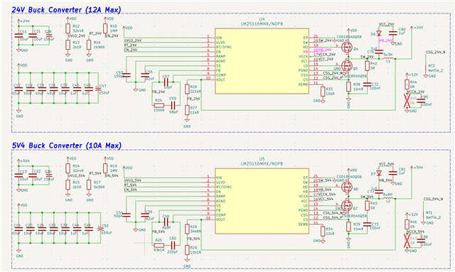
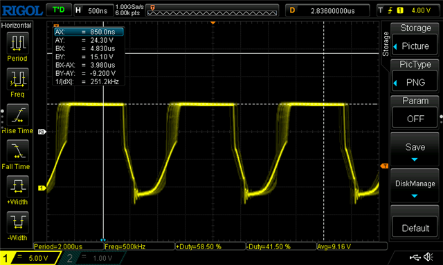
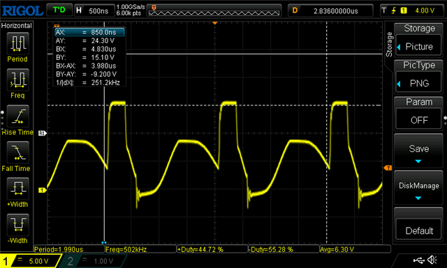
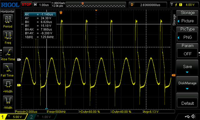
I am having some trouble with my LM25116 buck converter design.I have two LM25116 ICs on my PCB. Both of them need to be able to handle an input range of 25V - 33V2. One of them has an output voltage of 24V with a switching frequency of 1MHz and the other has a output voltage of 5V4 operating at 500kHz. Both of their VCCs are powered by another small buck converter LMZM23600SILT with an output voltage of 12V. The 24V LM25116 does not seem to be regulating the voltage at all. The voltage at the feedback pin varies as the input voltage changes. All the solder joints look good but the duty cycle remains at 70% regardless of the input voltage. However, with the almost identical design, the 5V4 regulator does not seem to suffer this issue. But there is a huge gate ringing issue once the input voltage is around 8V. I have attached the schematics below. Also, I would like to discuss this issue further in private. I have attached the schematics below.

  • Hi Robin,

    1st converter: Vin=25V-33V, Vout=24V. The maximum allowable switching frequency with the above condition is ~50kHz-60kHz, but you are trying to operate at 250kHZ which the device won't be able to regulate. Please use design tool properly to avoid such schematic issues: LM5116-5116WG-25116DESIGN-CALC Calculation tool | TI.com

    Operations with low input voltage (~25V_vin_min) requires a high a very high duty cycle [ at Vout=24V] to maintain Vout regulation. The maximum possible duty cycle is limited by minimum HO off-time required for sampling DC inductor current. The output will fail to regulate if the following condition is not satisfied

    Fsw<(Vout-Vin_min)/(Vin_min*580ns)

    Regards

    Arpita

  • Hi Arpita,

    Thank you for your reply. I was wondering if you could point out where I can find the maximum operating frequency on the datasheet. When I was checking the datasheet, I only noticed that the switching frequency would be limited when VCCX is less than 6V but right now the VCCX is powered by a 12V buck converter so I am slightly confused why I could only operate at 50kHz-60kHz. Also, the 5V4 line is running at 500kHz and the 24V rail is at 1MHz. So im not sure where the 250kHz is coming from .

  • Also would it possible to continue this conversation in private such as by emails?Thanks

  • Fsw<(Vout-Vin_min)/(Vin_min*580ns)

    Als, i think the equations is incorrect. Vout is alwasy smaller than Vin. Having a negative frequency wont make too much sense

  • Also according to my calc, the absolute minimum Fsw would be 130kHz for my 24MHz buck converter asssuming the lowest input votage is 24V.

    • Fsw <= 7.14MHz=Vout/ Vin_max * 100ns = 24V/(33.6V*100ns) 
    • Fsw <= 133kHz=(Vin_min-Vout)/ Vin_min * 580ns = (26V-24V)/(24V*580ns)

    Running at 500kHz shouldnt be a problem for the 5V4 buck:  

    • Fsw <=1.61MHz=Vout/ Vin_max * 100ns =5.4V/(33.6V*100ns) 
    • Fsw <= 1.36MHz=(Vin_min-Vout)/ Vin_min * 580ns = (26V-5.4V)/(24V*580ns) 
  • In addition, although the 5v4 buck converter is properly regulating the output voltage, its gate(HO pin19) voltage is behaving weird. 

    With a 7.9V input voltage, the node seems okay with some ringing at the falling edge.


    However, as soon as the input goes to 8V, the gate node has a completely different waveform.

    At 13V the node goes wild but sill have a similar shape the the 8V waveform.


    Keeping increasing the input voltage would not change the general shape from now on. It will only make the spike higher and narrower. The switching node also resembles a similar shape. Note that there is no gate snubber populated right now. What could cause such behavior and should i be concerned? Is there any way to resolve this issue? The output voltage seems totally fine. 

  • Hi Robin,

    In datasheet, the Forced HO off-time and Minimum HO on-times are given. Let's understand that the switching frequency [for a given application case of Vin, Vout] has to be chosen such that these limitations does not hit. You can calculate the maximum possible switching frequency for a given Vin, Vout from these. 

    However, you can directly use the excel tool which has been already shared to you. You will get proper explanation and equations in the excel itself for easier calculation.


    As for 1st converter: Vin=25V, Vout=24V, D~0.96, at Fsw=1Mhz [current value set] gives a required off-time of ~40ns where as the forced HO off time iof the device is 580ns. Hope this makes it clear.

    VCCX sets the maximum possible oscillator frequency. But while setting operating switching frequency, the above points have to be taken into account.

    Regards

    Arpita

  • Sorry for the Typo, it is clearly Fsw< (Vin_min-Vout)/ (Vin_min*580ns) 

  • Yes 2nd converter is fine 5.4V

    For first converter:

    Fsw <= 133kHz=(Vin_min-Vout)/ Vin_min * 580ns = (26V-24V)/(24V*580ns)

     Vin_min=25V, Vout=24V for your case

    So the correct calculation should be fsw<(25-24)/(25*580ns) which comes out to be Fsw~60kHz. I have suggested to use 50kHz-60kHz for 1st converter.

  • 2nd converter:  What is the load current when you have captured this? I think as the load current is less, so the device is in DCM mode, as you are probing HO_GND, the DCM ringing at SW node appears in HO_GND also.

    To check gate voltage of top Mosfet properly, gate to source voltage should be probed i.e. HO_SW.

    Regards

    Arpita

  • Thanks for the suggestion. The ho_sw is looking a lot like a square wave but why does the SW mode looks like its having three states, which seems like its in dcm mode. i already put a 10k resistor at demb pin so it should be in full sync mode?

  • Can you please try changing the DEMB resistor value and recheck?

    Also try using increasing load current

    Regards

    Arpita

  • Thank you very much again for your reply. I was wondering if you have an email address I could reach you at. I have a video I would like to share, but due to confidentiality and IP considerations, we would prefer not to post it publicly here. I truly appreciate your time and understanding, and I look forward to hearing from you.

  • Hi Robin,

    Kindly accept the request to message privately in the forum.

    Regards

    Arpita