UCC5390: UCC5390SCDR

Part Number: UCC5390

Tool/software:

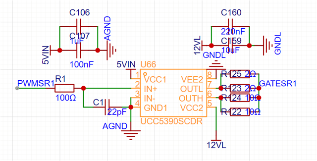
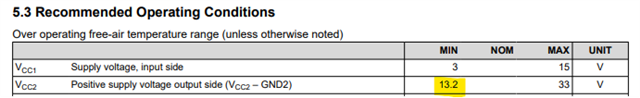
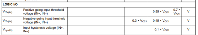
When I use UCC5390SCDR to drive MOS, VCC1 pin is powered by 5V, IN- pin is directly connected to GND1 pin, VCC2 pin is powered by 15V, and VEE2 is 0V,and my controller is stm32G474 seires and I can detect the 3.3Vpwm from the IN+ pin. However there is no output at the OUT L/H pin. At this time, the primary side power loss is 0.01W, and the secondary side loss is 0.03W. I would like to ask what might be the situation, what methods can I use to determine the problem, and how can I correct these issues?

  • Hi Pengfei,

    Did it work before? This could be the result of damage. The first thing I would try in that case is to replace the gate driver and check OUT and Vgs for excessive noise. 

    The UCC5390 has a 12V under-voltage lock-out (UVLO) that will turn the gate driver OFF for voltages below 11V. The VCC2 net label in your schematic is 12VL, but you wrote 15V. Can you confirm the voltage between VCC2 and VEE2? The minimum recommended is 13.2V:

    Also, a 3.3V input signal with a 5V input supply is not a good combination for this gate driver. The UCC5390 input logic thresholds are set to a ratio of VCC1: 

    With a 5V supply, the positive going input threshold is 0.55*5V=2.75V. This is less noise margin than if you use VCC1=3.3V. 

    Also, you have routed the input trace under the gate driver. Are you sure you need to use an isolated gate driver? This is forbidden when you need to maximize creepage anc clearance to support a high voltage between the input and output sides of the UCC5390.

    Best regards,

    Sean

  • Hi Sean,
    Thank you for answering my question. After replacing the gate driver, the circuit works normally now.
    Best wishes,
    Pengfei