LM5180: CMTI mitigation

Part Number: LM5180

Tool/software:

Good morning,

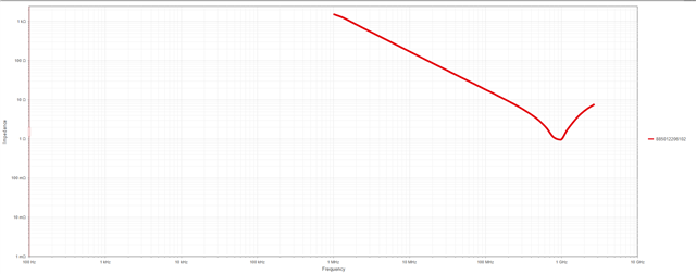
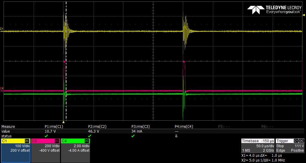
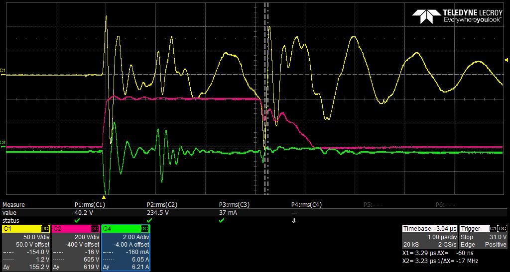
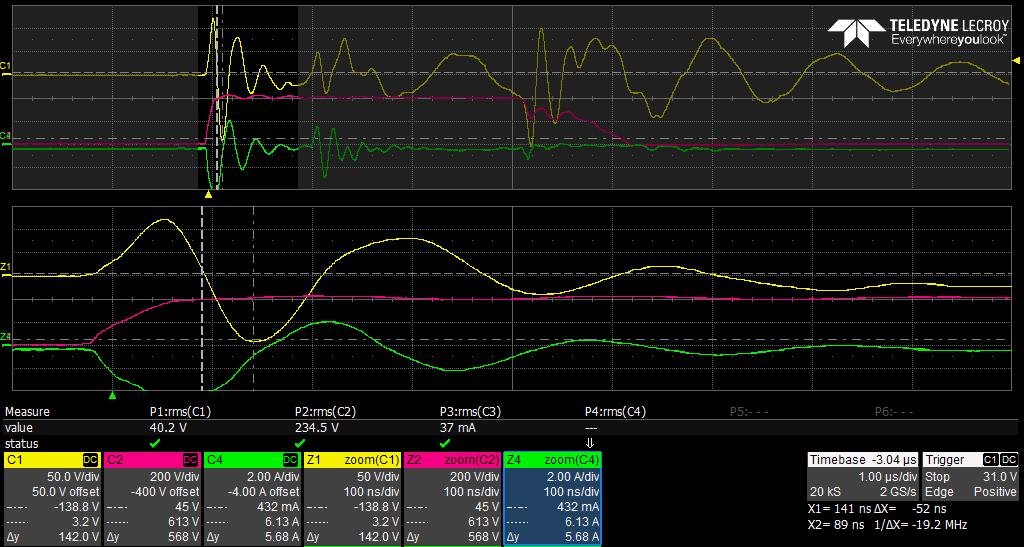
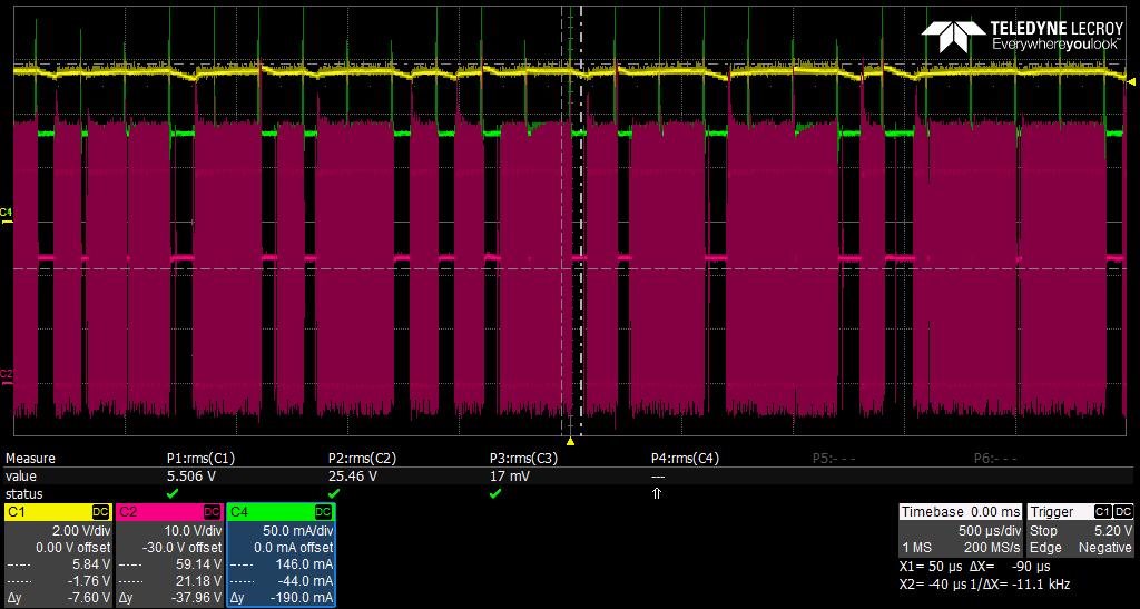
I am experiencing CMTI in my PSR Flyback, and I would like to know how to mitigate this problem. I have read SSZTD09, which talks about this topic, but it does not explain how to design the two filters, the RC one on the SW pin and the capacitor in parallel with Rset. 

How should I design these components? Are there any other strategies I could adopt to mitigate the problem?

Kind regards,

Davide

  • Davide,

    You can design the capacitance based on the SRF (self-resonant frequency) of the capacitor. The SRF shall be larger or slightly higher than the CM frequency. As an example, an 100pF, 100V, X7R, 0603, PN: 885012206102 has an SRF ~900MHz (see below), meaning that at that frequency it provides a low impedance path to the CM currents flowing across the isolated grounds. In order to know the frequency of the CM currents, what you can do is to measure the ground bounce voltage across the isolated ground with a voltage probe and take the FFT (frequency response) in the scope. What most of customer do is to start with an estimated value (such as 100pF) and check the improvements adn from there they adjust to higher or lower capacitance.

    Regarding the resistance value, it is recommended to select a small value compared to RFB so that Vout regulation DC does not change much.

    Thank you

  • Hello Manuel,

    measure the ground bounce voltage across the isolated ground with a voltage probe

    I have measured the voltage between the secondary winding ground and the primary ground using a differential probe, and this is the result:

    C1 channel shows the voltage between the secondary and the primary ground

    C2 channel shows the phase motor voltage with respect to -HV

    C4 channel shows the current on the phase motor

    The application is an inverter drive with an IGBT module, whose commutation frequency is 5kHz, and the DC bus voltage is 400V.

    The next image is a zoom of the first one. It better shows the signal I have between the grounds.

    While the next image shows the ground voltage rising edge.

    Then I can show you the effect of this CM noise on the Flyback regulation.

    C1 channel shows the secondary winding DC output voltage

    C2 channel shows the reflected secondary voltage

    C4 channel shows the secondary winding output current

    How could I filter this signal, or increase the circuit immunity to this noise, without compromising the Flyback regulation?

    Davide

  • Hi,

    The team is out of office today on U.S. holiday. We will get back to you soon.

    Thank you for your patience.

    Regards,

    Max Verboncoeur

  • Davide,

    -Please, send me your layout to be reviewed. We need to check the switching loop on both sides, the FB regulation loop and the ground planes locations.

    -Add an RC filter between VIN and FB pins. Start with a 100ohm+100pF.

    Thank you

  • Hello Manuel,

    I need time to prepare the information you need to help me with the layout design.

    In the meantime, could you suggest a diode I can use in the place of the CMDD4448 used in the evaluation board that is in a SOD323 package? It would help me to optimise the layout even better.

    Thank you,

    Davide Tosatto

  • Hi Davide,

    You can use an Schottky diode with 100V reverse voltage and 1A bias current.

    Thank you