Tool/software:
Hi Team,
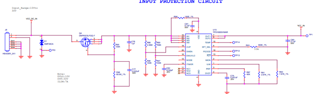
We are using this part in our design. TPS16850VMAR
Could you confirm whether the following pins can be left unconnected? or is there any necessary circuits to be added.
Our requirement: 10V-30V input range and 7A current.
UVLO= 10, OVLO-30V, ILIM - 7A
1) Fault: added testpoint for debugging
2) PGOOD:
3) Temp
4) FLT:
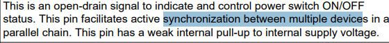
5) SWEN
Also, let us know shall we share the schematic for review
Thanks in advance
Regards,
Sathya Priya N.