TPS6594-Q1: PMIC EN_DRV

Part Number: TPS6594-Q1

Tool/software:

Hello,

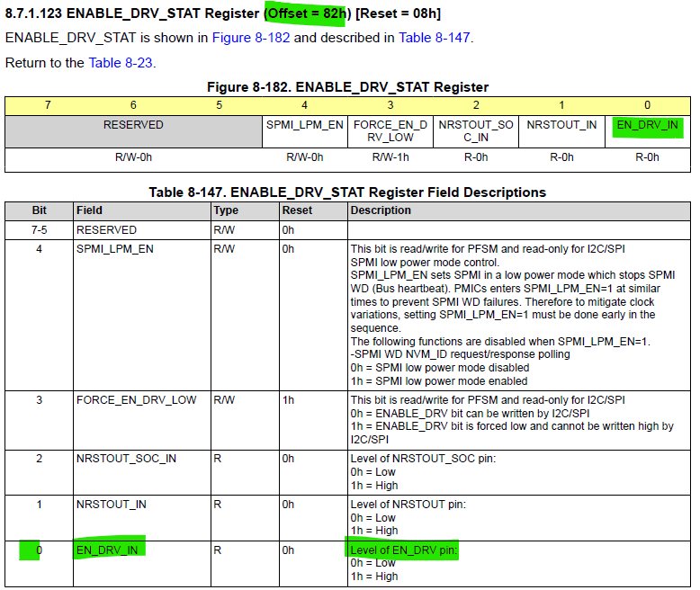
I am using TPS6594-Q1. I want to read the pin EN_DRV. 

Current trying to read this register after initializing the PMIC WD(WD is activated, configured window1, window2 and long window times).

How can I read this pin? what should be the slave address if I want to read this pin. Which register has to be read to read the status of this pin?

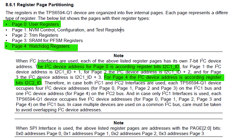
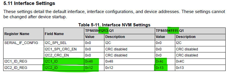
note: I am using I2C bus to read PMIC register

Kind regards

Thanks

  • Hi Manisha,

    Which long part number/OPN of the TPS6594-Q1 are you using, as this can affect the slave address so can change the answer. E.g. TPS6594133A. 

    The EN_DRV pin level can be read from the ENABLE_DRV_STAT register (offset 82h), specifically bit 0 is for EN_DRV_IN - you can see this in the device datasheet https://www.ti.com/lit/gpn/tps6594-q1 section 8.7.1.123 ENABLE_DRV_STAT Register:

    For address, this is register 82h. For I2C address, see the datasheet section 8.6.1 Register Page Partitioning. This explains the various pages of registers and how this interacts with the I2C address. Importantly for your case, the watchdog registers are on page 4, and the user registers (including ENABLE_DRV_STAT) are on page 0. Depending on the configuration of the device used (which is why I ask about long part number), these are often even on different I2C interfaces, I2C1 for user registers vs I2C2 for watchdog. This could cause an issue if you have not been taking this into consideration. You can find the I2C1_ID and I2C2_ID in the user's guide for the particular PMIC variant you are using. 

    The final thing you will need to consider is whether CRC is enabled on the I2C or not, and that you are correctly sending that if it is enabled. 

    I hope this helps - let us know the full part number and we could answer more specifically if there is still confusion. 

    Regards,

    Katie

  • Hello Katie,

    Thanks for the detailed explanation. The current OPN for PMIC A is "TPS65941213RWERQ1" and PMIC B is TPS65941111RWERQ1. Does this register (0x80) is connected to different I2C interface?
    WD is connected to MCU domain of I2C. Give me more details about it? 

    Thanks 
    Regards
    Manisha N G

  • Hi Manisha,

    For TPS65941213 and TPS65941111 you can refer to the user's guide Optimized TPS65941213-Q1 and TPS65941111-Q1 PMIC
    User Guide for JacintoTm 7 J721E, PDN-0C https://www.ti.com/lit/pdf/slvuc99 for more details about the specific config. In section 5.11 Interface settings you will find the I2C1_ID_REG and I2C2_ID_REG, which are the base I2C addresses for I2C1 and I2C2 on these devices, as well as that CRC is disabled at startup: 

    This device uses separate I2C interface, I2C2 on the PMIC, for the watchdog only. So using this information and the datasheet information in previous post, you can use the following as your I2C interfaces and addresses:

    TPS65941213-Q1: 

    • User register writes = page 0: use PMIC I2C1 interface, with 0x48 as the I2C address
    • Watchdog registers = page 4: Use PMIC I2C2 interface, with 0x12 as the I2C address

    TPS65941211-Q1:

    • User register writes = page 0: use PMIC I2C1 interface, with 0x4C as the I2C address
    • Watchdog registers: N/A as this is the secondary device and has watchdog disabled (see user's guide section 5.13 Watchdog settings). 

    And for the connections between PMIC I2C1 and PMIC I2C2 and the different I2C interfaces on the Processor, see the same user's guide, Figure 3-2 TPS6594-Q1 Digital connections. Note that in this example PDN, EN_DRV pin is not used but is available (so you could use it if needed in your own design). 

    So back to EN_DRV status read, you would read ENABLE_DRV_STAT register on I2C1 interface lines, with I2C1 address 0x48, and then use register address 0x82.

    Regards,

    Katie

  • Hello Katie,

    Thanks for the information. I am trying to read the status of EN_DRV pin from the register ENABLE_DRV_STAT and ENABLE_DRV_REG. What is the prerequisite for setting EN_DRV pin high? . I cross checked that FORCE_EN_DRV_LOW(bit 3) of  ENABLE_DRV_STAT is also set to low. 

    Thanks

    Manisha N G

  • Hello Katie,

    Thanks for the information. I am trying to read the status of EN_DRV pin from the register ENABLE_DRV_REG. What is the prerequisite for setting EN_DRV pin high in window1? .

    After I disable the WD and clear all the interrupts EN_DRV pin can be set to high. But when I check the status of the pin EN_DRV in Window1, this pin is always read to 0.

    How can the EN_DRV pin be set to high when WD is out of long window?

    The WD_FAIL_CNT_REG Register  is 0.

    Thanks

    Manisha N G

  • Hello all,
    I am studying the behaiviour of EN_DRV pin. This pin is configurable when WD is disabled. But on enabling WD, EN_DRV pin is set to low by HW. Before enabling WD, I made sure that there are interrupts in INT_TOP Register and INT_MISC Register. Also NSLEEPB[0] & NSLEEPB[1] bits in register FSM_NSLEEP_TRIGGERS (0x86) are set to 1.
    Why I am observing EN_DRV bit value as 0.
    Expectation is,
    once WD is out of long window, MCU must be able to change the pin value in window1.
    This is also not possible. Writing to this pin has no effect. Can expert clarify on this topic

    Thanks

  • Hi Manisha,

    Going through the checklist from the FAQ vs what you described - do you also disable the ESM before you do this? Both ESM and WD have to be handled. 

    Additionally, can you share a screenshot or scope shot or code snippet of the I2C write you are using to set the EN_DRV, as well as the specific sequence of WD writes that you perform for doing the config, so that we can check it? 

    Regards,

    Katie

  • Hello Katie,

    Due to NDA I cannot disclose the code, but I can share the sequence of the code.

    - Disable WD

    - Read the 0x5A and 0x6C on Page 0

    - There were interrupts in 0x5A which is MISC_INT and STARTUP_INT (bit 4 and 3 respectively)

    - INT_MISC (0x66) register is cleared and ENABLE_INT (bit 1) of INT_STARTUP(0x65) is set to 1

    Set NSLEEPB[0] & NSLEEPB[1] bits in register FSM_NSLEEP_TRIGGERS (0x86) to 1 as suggested in one of E2E threads for enabling EN_DRV pin

    - WD_PWRHOLD bit WD_MODE_REG register is cleared

    - Enable WD

    - Trying to enable EN_DRV pin (setting ENABLE_DRV (bit 0) of ENABLE_DRV_REG Register)

    • When can this bit be set (in window1 or widnow2) if at all it is possible to set by MCU?

    • The value of ESM_MCU_EN of  ESM_MCU_MODE_CFG Register is 0, hence I did not write separate instruction to disable ESM.

    Thanks

  • Hello Manisha,

    Due to national holiday in US, most of the experts are out of office today. Please expect delay in response. Thanks for your patience!

    Regards,

    Ishtiaque

  • Hello Experts,

    I am able to set EN_DRV pin at the end of window2 but not in window1
    can you please explain this behaviors

    Thanks
    Manisha N G

  • Hi Manisha,

    You also need WD_FIRST_OK=1, so you need to have gone through the window-1 and window-2 completely once first so that this will be set. I would refer to Figure 8-27 Flow Chart for WatchDog in Q&A Mode from the TPS6594-Q1 datasheet. This flowchart also shows that only after window-2 completes and no WD_BAD_EVENT will the ENABLE_DRV be able to be set to 1 (see box in the very bottom right corner of chart). 

    Regards,

    Katie

  • Thanks Katie for confirming this behavior.