UCC15241-Q1: design calculation excel

Part Number: UCC15241-Q1
Other Parts Discussed in Thread: ISO5852S

Tool/software:

Hello experts:

we have some questions regarding the design calculation Excel sheet "UCC1524x-Q1_Calculator_V8 (*1)."

We apologize for the many questions, but we would appreciate it if you could respond.

Best regards,

Zhou

[Assumptions]

 * Input Voltage: 24V

 * Output Voltage: 18 V/-2 V (Dual output)

 * Application: Power device driving gate driver power supply

[Questions]

  1. Understanding of Input Cells and Output Cells

I understand that the user inputs values in the green cells, and the output appears in the white cells. Is my understanding correct that filling in all the green cells completes the design (circuit constants only)?

  1. Regarding C_OUT1B on line 48, and C_OUT2 and C_OUT3 on lines 51 and 53 2-1) Can I assume that the calculation results on lines 48, 50, and 52 in the Excel sheet represent the minimum required capacitance, and it is acceptable to select components with larger capacitance?

2-2) Is my understanding correct that we are seeking the minimum value of the black line in Figure 12-5 of the datasheet (*2)?

2-3) It seems that changing the Max. component tolerance values inputted on lines 25 to 29 of the Excel sheet does not affect the calculation results on lines 48, 50, and 52. Does this mean that these results do not include tolerance, and we need to consider tolerance when selecting actual capacitor components?

2-4) I believe that for C_OUT2(MIN) and C_OUT3(MIN), we need to select capacitors with capacitance larger than these values. However, if we select a capacitor that exceeds the calculated capacitance due to a -20% tolerance, and the actual capacitance is +20%, would that result in a total capacitance of +40% compared to the calculated result still be acceptable?

2-5) As mentioned earlier, since the calculation results for COUT2 and COUT3 are marked with (MIN), selecting components with capacitance larger than the calculated results will change the ratio of COUT2 to COUT3. Is that a problem?

2-6) The datasheet Table 12-2 states, "The COUT2 and COUT3 capacitance ratio is important to optimize the dual output voltage divider accuracy." Is there a method to calculate the output voltage variation? For example, if we select capacitors with capacitance larger than the results on lines 50 and 52, the ratio of COUT2 to COUT3 will change from the calculated results. How can we calculate the impact on the output voltage?

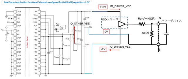
  1. Regarding the currents from lines 17 to 20

I recognize the meanings of each variable as shown in the attached image, is that correct? If I am mistaken, I would appreciate your guidance on those points.

 * IQ_DRIVER_VDD and IQ_DRIVER_VEE: Current consumption on the gate driver circuit side (excluding the switching current flowing through Rg in the attached image and the current flowing through 10kΩ)

(Example: When using ISO5852S, IQ_DRIVER_VDD = IQ_DRIVER_VEE = ISO5852S's Output-supply quiescent current (max) 6mA)

 * IQ_OTHER_VDD: Current flowing through RFBVDD_VEE and RFBVDD_VDD

 * IQ_OTHER_VEE: None (0A)

  1. Regarding RFBVDD_VEE and RFBVEE_VDD on lines 23 and 24 As stated on page 38 of the datasheet, is it acceptable for RFBVDD_VEE=10k and RFBVEE_COM=10k to remain constant at 10kΩ regardless of design values such as output voltage? I understand this is for the filter formed with the 330pF capacitor. In this design, since the voltage between VEE and COM will be less than 2.5V, I plan to adjust the resistance value on line 24 to bring RFBVEE_COM closer to 10kΩ.
  2. Regarding the determination of power input values on lines 37 and 39 I could not find the SOA curve (*2) corresponding to the desired output voltage of 18V/-2V in the datasheet. If there is an SOA curve for 18V/-2V, could you please provide it? If you cannot provide the SOA curve for 18V/-2V, could you suggest an alternative design method (e.g., using the SOA curve values for 18V/-5V)?
  3. Regarding the impact of power input values on the design on lines 37 and 39

 * If the value on line 37 is small, the cells from lines 13 to 20 turn red. How should this be interpreted?

 * If the value on line 39 is small, how do the values on lines 48 to 52 change, and what calculations are being performed?

*1 Design calculation Excel sheet: https://www.ti.com/tool/download/UCC15241-Q1-CALC [https://www.ti.com/tool/download/UCC15241-Q1-CALC]

*2 Datasheet: https://www.ti.com/lit/ds/slusf14/slusf14.pdf?ts=1756166123483 [https://www.ti.com/lit/ds/slusf14/slusf14.pdf?ts=1756166123483]

*3 Evaluation board: https://www.ti.com/lit/ug/sluucj2c/sluucj2c.pdf?ts=1756097715366&ref_url=https%3A%2F%2Fwww.ti.com%2Ftool%2Fja-jp%2FUCC14240EVM-052 [https://www.ti.com/lit/ug/sluucj2c/sluucj2c.pdf?ts=1756097715366&ref_url=https%3A%2F%2Fwww.ti.com%2Ftool%2Fja-jp%2FUCC14240EVM-052

  • Zhou,

    These are some good questions, I appreciate your attention to detail. I will do some digging and get back to you with the answers by the end of the day tomorrow.

    Regards,

    Carter Pollan

  • Zhou,

    1)

    1. Understanding of Input Cells and Output Cells

    I understand that the user inputs values in the green cells, and the output appears in the white cells. Is my understanding correct that filling in all the green cells completes the design (circuit constants only)?

    The high level purpose of the calculator is to A) make sure that the requirements of your design can be met with this and B) give proper component ranges/values for all of the component  you will need in order to get this chip up and running. After you have completed the calculator all of the circuit components should be properly constrained as far as layout and component values.

    2)

    Regarding C_OUT1B on line 48, and C_OUT2 and C_OUT3 on lines 51 and 53 2-1) Can I assume that the calculation results on lines 48, 50, and 52 in the Excel sheet represent the minimum required capacitance, and it is acceptable to select components with larger capacitance?

    This is not true. The ratio between the capacitors is also critically important. Here is an excerpt from the datasheet:

    "Bulk charge, decoupling output capacitors are required to be located next to the gate driver pins. The COUT2 and COUT3 capacitance ratio is important to optimize the dual output voltage divider accuracy during charge or discharge switching cycles; while the COUT1B capacitor is used to minimize the total capacitance including COUT1B, COUT2 , and COUT3 capacitance values." page 31

    Following the guidelines in the calculator to choose the closest standard value but higher will make sure you avoid the problems with an unbalanced capacitance ratio. There is more information in section 12.2.2.1 on page 31 of the datasheet if you are interested.

    2-2)

    Is my understanding correct that we are seeking the minimum value of the black line in Figure 12-5 of the datasheet (*2)?

    Yes, that is correct.

    "The optimal COUT1B, COUT2, and COUT3 at the minimum total net capacitance benefit both output capacitor size reduction and BOM cost reduction." datasheet page 32

    2-3)

    It seems that changing the Max. component tolerance values inputted on lines 25 to 29 of the Excel sheet does not affect the calculation results on lines 48, 50, and 52. Does this mean that these results do not include tolerance, and we need to consider tolerance when selecting actual capacitor components?

    I would recommend using relatively tight tolerance resistors for this application. In your later comments you mention +/-20% capacitors. It is not recommended to use capacitors with that loose of tolerances in this application where precision is necessary. If you choose the closest standard value higher than the calculated value with a 5% resistor you will avoid all of the problems in questions 2-4 to 2-6.

    3)

    I recognize the meanings of each variable as shown in the attached image, is that correct? If I am mistaken, I would appreciate your guidance on those points.

    I would recommend adding up all of the quiescent currents in your system and adding them to line 17. That being said, your understanding of those currents is correct.

    4)

    Regarding RFBVDD_VEE and RFBVEE_VDD on lines 23 and 24 As stated on page 38 of the datasheet, is it acceptable for RFBVDD_VEE=10k and RFBVEE_COM=10k to remain constant at 10kΩ regardless of design values such as output voltage? I understand this is for the filter formed with the 330pF capacitor. In this design, since the voltage between VEE and COM will be less than 2.5V, I plan to adjust the resistance value on line 24 to bring RFBVEE_COM closer to 10kΩ.

    Yes, it would be fine to use 10K for both RFBVDD_VEE and RFBVEE_COM as long as the other half of the resistor divider is adjusted accordingly.

    5)

    Regarding the determination of power input values on lines 37 and 39 I could not find the SOA curve (*2) corresponding to the desired output voltage of 18V/-2V in the datasheet. If there is an SOA curve for 18V/-2V, could you please provide it? If you cannot provide the SOA curve for 18V/-2V, could you suggest an alternative design method (e.g., using the SOA curve values for 18V/-5V)?

    This SOA curve with VVDD-VEE=18V and VCOM-VEE=5V was preformed with no load on VCOM-VEE, so it will serve you well when designing with a 18V/-2V system.

    6-1)

    If the value on line 37 is small, the cells from lines 13 to 20 turn red. How should this be interpreted?

    This is asking you for the maximum recommended average power SOA area. It is not asking you for the average power that will be consumed by your design. You can find this by referencing the SOA curve I have above, or by referencing the ones in the calculator. You can find this value by finding the maximum value of the red dotted line on the SOA graph. In this case it will be 2.5. The calculator only gives errors if the value is below 2.2, which is lower than any use of the SOA curves.

    6-2)

    If the value on line 39 is small, how do the values on lines 48 to 52 change, and what calculations are being performed?

    Those equations can be found in the datasheet on page 33. Cout3 is solved for using equation 3, Cout2 is solved for using equation 8, and Cout1b is solved for using equation 7.

    The value on line 39 is based on the capability of the device, not on the system requirements. As a result it will always be in the 2.5-3.5 range and shouldn't be that small. It can be found using one of the solid lines in the SOA curves at 25 degrees C. Because you specified an input voltage of 24V your value will be about 3.

  • Thank you very much for your reply and details.

    We will try to understand this and if we have further questions, will ask you again.

    Best regards,

    Zhou