Tool/software:
I have designed a BMS circuit by using the reference diagram given in Data sheet, but the circuit is charging and balancing the batteries.But there is no discharge through the pack output pin. what will be cause?. 
Tool/software:
I have designed a BMS circuit by using the reference diagram given in Data sheet, but the circuit is charging and balancing the batteries.But there is no discharge through the pack output pin. what will be cause?. 
Can you provide the Register Settings and Status bits? I suspect there may be some fault or setting that is preventing the Discharge FET from turning on.
I'm not sure this is your issue but it is recommended to place an actual cell between the VC15-VC16 pins, while shorting any used pins with no cells. between VC2 to VC15.
"The BQ769x2 device family requires at least 3 cells at all times to operate. These cells must be placed in ascending order so that so that there are cells between VC0-VC1, VC1-VC2, and VC15-VC16." T
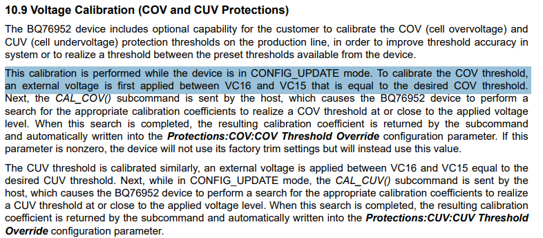
his may be because of how the Voltage calibration is done: "This calibration is performed while the device is in CONFIG_UPDATE mode. To calibrate the COV threshold, an external voltage is first applied between VC16 and VC15 that is equal to the desired COV threshold."

  bms.reset();
  delay(100);

  // Configure the BQ76952 just the way we like it:
  bms.setConnectedCells(6);

  bms.writeByteToMemory(CUV_Threshold, 70);
  bms.writeByteToMemory(COV_Threshold, 84);

  // Set OCD1 to 60mV across shunt (200A)
  bms.writeByteToMemory(OCD1_Threshold, 30);

  // Set SCD to 80 mV (265 A)
  bms.writeByteToMemory(SCD_Threshold, SCD_80);

  // Enable CUV, COV, Short circuit and OCD1 protection
  // bms.writeByteToMemory(Enabled_Protections_A, 0b10101100);
  bms.writeByteToMemory(Enabled_Protections_A, 0b11101100);

  // FET thermistor on DCHG. Enable FET + internal temp protections
  bms.writeByteToMemory(DCHG_Pin_Config, 0b00001111);
  bms.writeByteToMemory(Enabled_Protections_B, 0b11000000);

  // Report in centiamps (10mA),configure for 300uR shunt [default: 1mR]
  bms.writeByteToMemory(DA_Configuration, 0x06);
  bms.writeFloatToMemory(CC_Gain, 24.92267);
  bms.writeFloatToMemory(Capacity_Gain, 7433474.88);

  // This enables the Pre-discharge function (1600 ms, 2.5 v delta)
  bms.writeByteToMemory(FET_Predischarge_Timeout, 160);
  bms.writeByteToMemory(FET_Predischarge_Stop_Delta, 250);
  bms.writeByteToMemory(FET_Options, 0x1D);

  // Configures balancing parameters
  bms.writeIntToMemory(Cell_Balance_Min_Cell_V_Relaxed, 3300);
  bms.writeByteToMemory(Cell_Balance_Max_Cells, 6);
  bms.writeByteToMemory(Balancing_Configuration, 0b00000010);

  // Disables SLEEP, slow measurement speed when balancing to 1/8th
  bms.writeIntToMemory(Power_Config, 0b0010100010110010);

  // Exits manufacture mode. Allows BQ to enable FETs subject to protections
  bms.writeIntToMemory(Mfg_Status_Init, 0x0050);
  bms.setFET(ALL, ON);
Here is my Register configuration settings, please have a look
A couple issues with your Schematic/Settings that may be contributing to your issues.
1. The emitter of Q1 appears to be going straight to GND, instead of to the REGIN pin like it should. Thus, REGIN is just floating on the C14 cap to GND.
2. If REGIN is not correctly biased from Q1, then the REG1 output will not be correctly regulated as it is powered from REGIN.
3. From your provided register settings, the DCHG pin is configured as a FET temp input. But the schematic show the DCHG pin as floating, thus its possible this may be accidentally triggering temperature fault that disables the DSG FET.
4. From your register settings the PDSG pin is configured for Predischarge mode. But the schematic shows it as floating, thus you will not get any Predischarge functionality.
If the inrush current is too high without the predischarge function, you may be triggering an over current fault that disables DSG.
Please check if there are any safety faults triggered in the Status Registers. Flags showing which safety faults may be present are available through the 0x03 Safety Status A, 0x05 Safety Status B, and 0x07 Safety Status C commands, and their presence can generate an interrupt to a host processor on the ALERT pin.