


Tool/software:
Team,
In the layout guidelines here, there're three layers been implemented. For the RF emission, what're the suggestions of the PCB layers in UPS application?
Customer's EMI standard has to follow IEC 62040-2
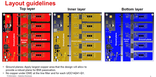
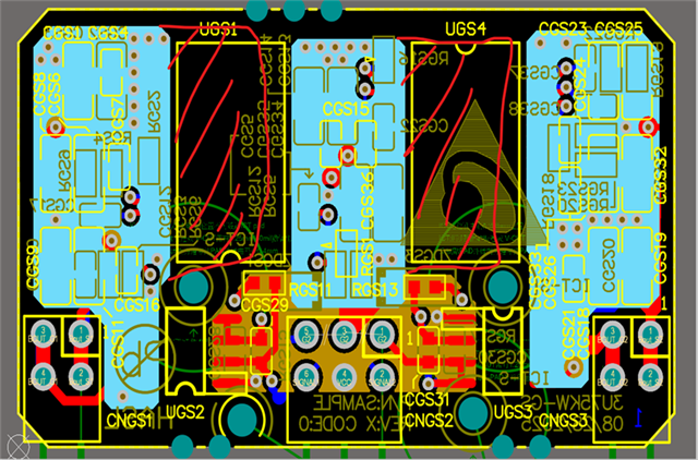
Here's customer's layout now. Blue color is ground plane, in the TI's layout guidelines, the copper areas of the inner layer is pour over to right side as red color mark.
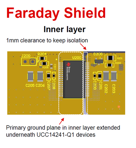
Larger copper areas act as shielding layers, effectively reducing unwanted RF interference. Is there any safety concern with Clearance? Is this suggested?
Guidelines for clearance to keep isolation:
Regards
Brian
