Tool/software:
hi expert
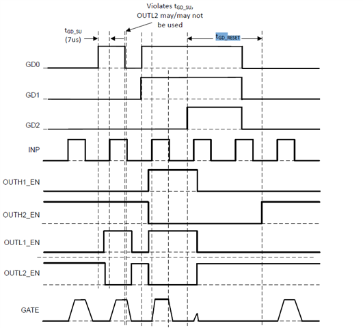
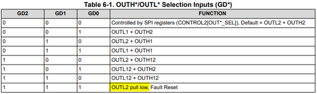
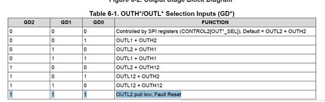
i saw the following table in our datasheet.
i want to know if GD=111, what is state of OUTH1/2 OUTL1? high impendence or others?
thanks
Hi,
The team is out of office today on U.S. holiday. We will get back to you soon.
Thank you for your patience.
Regards,
Max Verboncoeur
Hi Jay,
The output pins that are not enabled will be high impedance.
Regards,
Max Verboncoeur
ok got it thanks Max
i have a further question. i saw the following in datasheet.
Q1:what does GD_RESET mean? means that GD*=111?
Q2:according to this timing diagram, it seem that when GD*=111, The output pins are not high impedance?
could you can share your comments? thanks
Q3. adding another question.
assuming a situation:MCU control GD* pins of 6pcs 588X is 111b. and then MCU still send PWM to 6pcs 588x. at one moment, MCU send high pwm to one of GDIC, what is this GDIC output? high level or others?
Hi Jay,
Q1:what does GD_RESET mean? means that GD*=111?
GD*=111 triggers a reset of the fault registers. The t_GD_RESET is the time it takes for the gate driver to complete the fault reset process.
Q2:according to this timing diagram, it seem that when GD*=111, The output pins are not high impedance?
could you can share your comments?
The output pulls to OUTL2 when GD*=111.
Q3. adding another question.
assuming a situation:MCU control GD* pins of 6pcs 588X is 111b. and then MCU still send PWM to 6pcs 588x. at one moment, MCU send high pwm to one of GDIC, what is this GDIC output? high level or others?
You can see from the timing diagram, the GD*=111 takes priority over the INP signal and the output remains low. There is a little time between the GD overriding the PWM due to the 270ns deglitch on the GD pins.
Regards,
Max Verboncoeur