Tool/software:
Hello everyone,
I am new to this forum, so please excuse me if the formatting and writing do not follow all the rules.
I am working with an ESP32 (MCU) to read and write the BQ76952 via I2C.
I configured the BQ76952 so that it triggers predischarge (PDSG) when the DFETOFF pin is LOW.
Then, if the voltage difference between the LD pin and the PACK pin is below a threshold (the maximum), the DSG FET (discharge FET IO43) is active.
My configuration :
BQ76952 power supply:
- 12 V on BAT_pin (IO47)
- 35V VC16 (IO48)
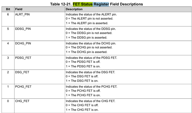
This seems to work according to the FET Status Register (0x7F) that I read:
- Phase 1: FET status register returns 97 (DEC) when DFETOFF HIGH.
measurement CHG FET: 23 V (active)
measurement DSG FET: 0V (not active)
measurement PCHG FET: 28V
measurement PDSG: 1.3V
- phase 2: FET status register returns 73 (DEC) when DEFETOFF LOW (Request predischarge).
CHG FET measurement: 23 V
DSG FET measurement: 0V
PCHG FET measurement: 28V
PDSG measurement: 1.3V
- Phase 3: FET status register returns 69 (DEC) when LD_pin reaches the value of PACK_pin.
CHG FET measurement: 23V (active)
DSG FET measurement: 23V (active)
PCHG FET measurement: 28V
PDSG measurement: 1.3V
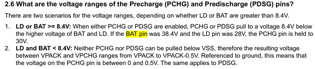
I use the PDSG pin to control a optocoupler to enable the precharge. I need 3,3V on the PDSG pin when he's active.
My questions are as follows:
- Should work the PDSG pin like the PCHG pin ? So is the output at 1.3V normal?
- Is it possible to configure the PDSG output voltage?
see below the FET status register :