TPS54A24: Damaged parts - Hole burned in package below pin 20

Part Number: TPS54A24

Tool/software:

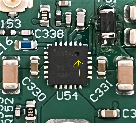
Hello, I have a TPS54A24 on a PCB design that is failing in the same way on several PCBs.  There is a small hole (~1mm diameter) that's burned in to the top of the package, near pin 20.

What is the typical cause for this type of failure?  Is it over current?  Is it overvoltage on the input?  Is is over voltage on the EN pin?

The input voltage is 15V, which is below the absolute max input voltage (19V).  However, the power supply providing the 15V has been unstable, and it's possible that the output voltage drifted higher for a short period of time.

Also, the EN pin is tied to VIN (15V), but I noticed that the absolute max rating for that pin is only 6.5V.  Would that cause the failure described above?

Thank you,
Owen 

  • Here is a photo of a damaged IC

  • Thanks Owen, I think you have likely debugged the issue. This is likely related to EN pin damage and that needs to definitely be fixed. It can also be related to the internal FETs if the VIN is not stable - any overvoltage on VIN and therefore SW (ringing + higher DC voltage) can also cause FET damage. If you would like, I can review your schematic and layout for correctness.

    Thanks,
    Amod

  • Thanks Amod.  After some more troubleshooting, I think I agree with you that it's the EN pin.  I managed to cut the trace on the PCB (since it had an internal pull up), and everything seems to be working fine.  Thanks again!