LMG1020EVM-006: How to maintain the output amplitude of SN74LVC1G08 in the LMG1020EVM-006?

Part Number: LMG1020EVM-006
Other Parts Discussed in Thread: SN74LVC1G08, LMG1020

Tool/software:

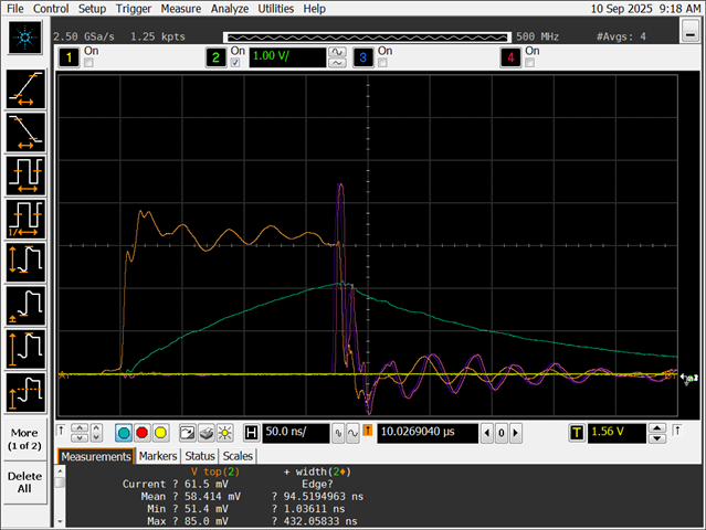
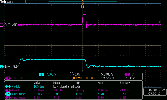
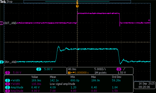
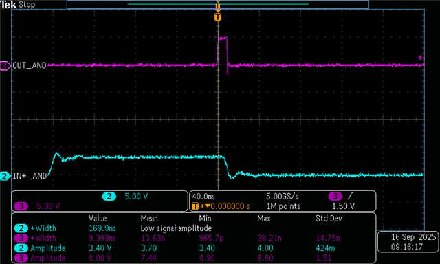
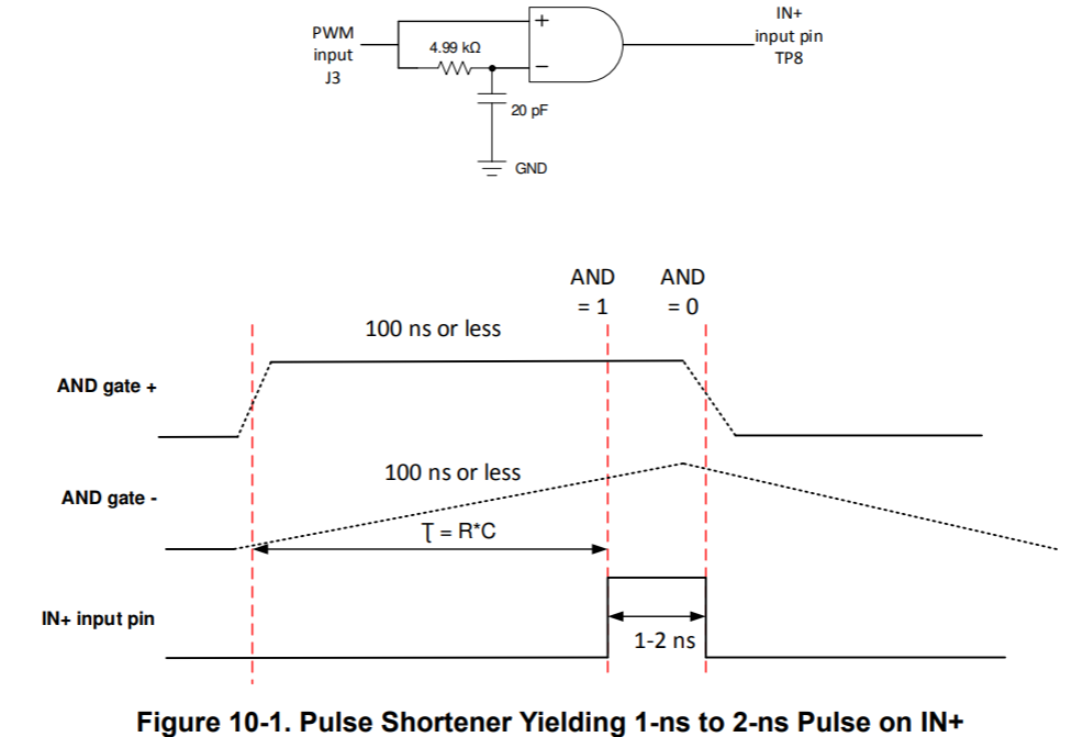
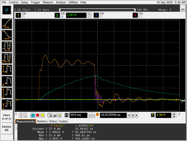
We use LMG1020EVM-006. This image is quoted from the EVM User's Guide: LMG1020EVM-006.We are adjusting the frequency of the function generator to achieve the narrowest possible pulse width (1 ns) at the output. 

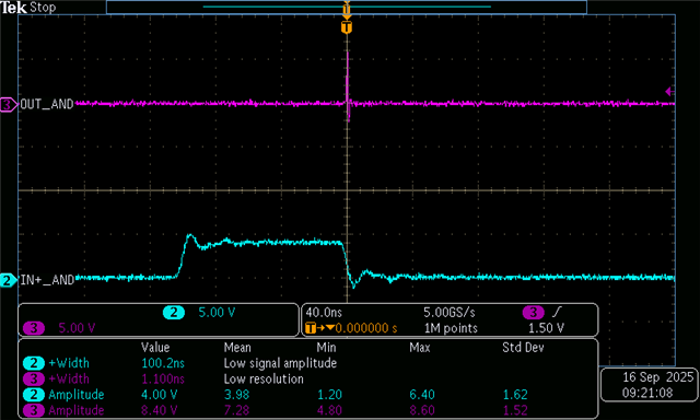
I would like to increase the output signal amplitude of the AND gate SN74LVC1G08 used in the LMG1020EVM-006 evaluation board.
The reason is that when trying to generate narrower pulses from the SN74LVC1G08, we found that the signal amplitude decreases.

How can we maintain the output amplitude while still generating narrow pulses from the SN74LVC1G08?

  • Hi Makiko,

    Is the LMG1020 still being triggered by the input pulse? The driver's input high threshold is 2.6V max, which the output of the AND gate should reach that with the 5V EVM supply. Can you tell me which components you have added or removed from the board since you opened it?

    Thanks,

    Annabelle

  • Dear Annablelle,

    Thank you for your reply! I appreciate it.

    I use LMG1020EVM-006 without any modifications. So, I input pulse into J3 on LMG1020EVM-006. The input pulse is about 100kHz or 250kHz. 

    Let me change the question. I would like to apply a higher voltage to the GaN-FET, so I want to maximize the amplitude of the output pulses from the LMG1020’s OUTL (OUTH). Based on our evaluations using the LMG1020EVM-006, it seemed that the amplitude of the signal input from the SN74LVC1G08 to the LMG1020 was proportional to the voltage at the LMG1020’s OUTL (OUTH).

    I would appreciate it if you could point out any mistakes. I would also be grateful for any advice.

    Thank you for your cooperation.

    Best regards,

    Makiko

  • Hi Makiko,

    The max recommended VDD is 5.4V, so the LMG1020 output cannot be higher in amplitude than that. And yes, the amplitude of the AND gate into LMG1020 will be proportional to the voltage at the LMG1020 OUT pins. So you cannot get any higher than that to drive the FET.

    What voltage level are you wanting to drive the GaN-FETs at?

    Thanks,

    Annabelle

  • Dear Annabelle,

    Thank you for your explanation!

    I want to drive the GaN-FET at over 4V, but as the pulse width approaches 1ns, the amplitude decreases, and currently only about 1V amplitude is being produced.

    I am also considering placing a buffer IC before the driver IC, which is after the AND gate. I am looking for a buffer IC that can operate at high speed, specifically around 1ns. Do you have any recommended products? Additionally, if you have any other suggestions, I would appreciate your advice.

    Thank you!

    Makiko

  • Hi Makiko,

    Do you mean that the output of the AND gate is only reaching 1V, or the output of the driver is only reaching 1V? Because the driver only requires 1.8V for the input high threshold, and then the output of the driver will provide the 5V to the FET. 

    Another note is that when using the AND gate as a pulse shortener, the slew rate is at the maximum, so the output pulses will be rounded and not have sharp edges and is rounded at the top.

    Could you please send a scope shot of the behavior you are seeing, including the IN+ and IN- to the AND gate, the output of the AND gate, and the output of the driver? Please use tip and barrel probe method to do so if possible. 

    Thanks,

    Annabelle

  • Hi  Annablle,

    Thank you for your reply! 

    Do you mean that the output of the AND gate is only reaching 1V, or the output of the driver is only reaching 1V?

    Yes. 

    Because the driver only requires 1.8V for the input high threshold, and then the output of the driver will provide the 5V to the FET. 

    I understand that the driver requires 1.8V for its input.

    Could you please send a scope shot of the behavior you are seeing, including the IN+ and IN- to the AND gate, the output of the AND gate, and the output of the driver? Please use tip and barrel probe method to do so if possible. 

    For comparison, I upload the waveform when the pulse width is adjusted to 2 ns (left) and when it is adjusted to 7 ns (right). The pink waveform represents the output from the driver, but at 2 ns the amplitude is lower. I would like to make this amplitude about the same as it is at 7 ns. I would greatly appreciate your advice!

    IN+ to the AND gate: orange

    IN- to the AND gate: dark green

    output  of the AND gate: purple

    output of the driver: pink

    [pulse width:2ns]                                                                        [pulse width:7ns]

     [  

    Best regards,

    Makiko

  • Hi Makiko, 

    I am going to test a new LMG1020 EVM in the lab to see if I can replicate the behavior you are seeing. Could you please provide me with your VDD, VIN level, switching frequency, and settings for IN+ and IN- pulses? And what did you populate the resistor load/laser diode space with? I will be out of office tomorrow afternoon and Friday, so I will complete this as soon as possible (likely early next week) once I have this information from you.

    Thanks for your patience,

    Annabelle

  • Dear Annabelle,

    Thank you for your cooperation! I have outlined the conditions below. I sincerely appreciate your willingness to conduct the reproduction test. I look forward to hearing from you next week.

    VDD of LMG1020, SN74LVC1G08     ->5V
    VIN level to J1 of LMG1020EVM-006   ->10V

    switching frequency  ->250kHz
    settings for IN+ and IN- pulses?    ->3.3V, pulse width about 170ns as shown in the figure above.
    what did you populate the resistor load/laser diode space with?  -> I use laser diode.

    Best regards,

    Makiko

  • Hi Makiko,

    Thanks for this information. Annabelle is out of office and expected to return on Monday, the 15th of September. Thank you for your patience.

    Best,

    Amy

  • Hi Makiko,

    Looking at the EVM user guide, the pulse width into IN+ of the AND gate should start at 100ns and slowly decrease until you get to the desired pulse width. Your waveforms seem to have the same 170ns pulse width for IN+ of the AND gate, but somehow you produced both a 7ns pulse and a 2ns pulse with it.

    When I recreated your setup, I did not see this same issue. I was able to achieve a 1ns pulse from the AND gate that reached 6V.

    You can find the EVM user guide here. I would recommend removing the laser diode and following these steps to correctly size the pulse width using a resistive load before adding the diode. I followed these steps based on the EVM user guide once taking the EVM out of the box. You said you had made no changes to the EVM besides adding the laser diode, so you should be able to do so even though you have used the EVM already. Quoted portions below are taken directly from the user manual.

    1. Check the effective resistance of your laser diode so you can effectively recreate it. "When selecting a resistor load, use 4 parallel 0603 size, 100 mW resistors and a typical laser diode resistance value of 1 Ω to 20 Ω. To achieve nanosecond pulses, a 1 Ω resistor load is recommended, in which four 4 Ω parallel resistors for R5 - R8 would be needed." I used four 4Ohm resistors. 

    2. "Start by testing the EVM without a bus voltage to achieve the required pulse width, frequency, and repetition rate on the gate test point, Vg (TP4)." The conditions should be as follows below: 

    - J1's DC bias supply should be at least 5.5 V, with current limited to 100mA. 
    - Function generator should be set at 0-3V, 100kHz, 100ns pulse width (I ended up increasing the input level from your setting of 0-3.3V because the SN74LVC1G08's high-level input voltage threshold at 5.5V is 3.85V, so you may have to do the same)

    3.  "When first starting to fine tune the function generator input to see the pulse on IN+, start with 100 ns then reduce the pulse width down by the nanosecond or smaller to make 1-2 ns visible on the IN+ test point." Please use tip and barrel to measure the IN+ and Vg test points (as shown below)

    4. Take the resistors, R5-R8, off before populating the laser diode

    Once you have tried this, please let me know if you are still experiencing this issue on the output of the AND gate. 

    Thanks,

    Annabelle

  • Dear Annabelle,

    I greatly appreciate your kind cooperation, and thank you for the information.

    I have one additional question: Could you please let me know the model name of the function generator you used in the test?Additionally, it would be helpful if you could let us know whether the output impedance of the function generator was set to 50 Ω or high impedance.

    Best regards,

    Makiko

  • Hi Makiko,

    The model name is Tektronix AFG3102C.

    For the output impedance, it was set to 50Ohm when I got the normal results. When I changed the setting to high impedance, I was not able to get a nanosecond pulse. Please see the images and conditions below:

    50Ohm, FG set at high of 2.2V, pulse width of 100ns: 1ns pulse

    50Ohm, FG set at high of 1.65V, pulse width of 170ns: 9ns pulse

    50Ohm, FG set at high of 3.3V, pulse width of 170ns: 116ns pulse

    High Z, FG set at high of 3.3V, pulse width of 170ns: 9ns pulse

    High Z, FG set at high of 3.3V, pulse width of 100ns: no pulse

    Thanks,

    Annabelle

  • Dear Annabelle,

    Thank you very much for providing such valuable information. I now understand that the load impedance of the function generator should be set to 50 ohms.

    (The output pin impedance of the function generator was fixed at 50 ohms. What I had checked was actually the load impedance setting. Please allow me to make this correction here.)

    In that case, may I ask if R4 (DNP) 50 ohms, located near J3 on the EVB, is populated?

    Thank you for your cooperation.

    Best regards,

    Makiko

  • Hi Makiko,

    No, R4 was not populated.

    Thanks,

    Annabelle