


Other Parts Discussed in Thread: BQ25798
Tool/software:
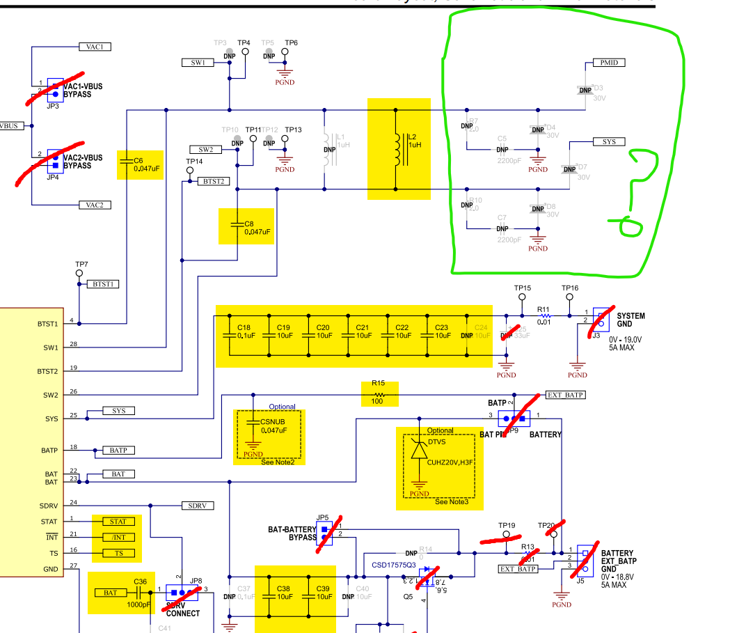
I am referencing the evaluation kit for the BQ25798 and designing my own PCB from it, and I am confused on what these components, circled in green, are potentially used for
Thank you!
Tool/software:
I am referencing the evaluation kit for the BQ25798 and designing my own PCB from it, and I am confused on what these components, circled in green, are potentially used for
Thank you!
