BQ25858-Q1: Automotive BMS

Part Number: BQ25858-Q1

Tool/software:

Technical Inquiries Regarding BQ25858-Q1 During Schematic and BOM Cost Evaluation​

We are currently in the schematic and BOM cost evaluation phase for a project using the BQ25858. We have several technical questions and would appreciate your advice:

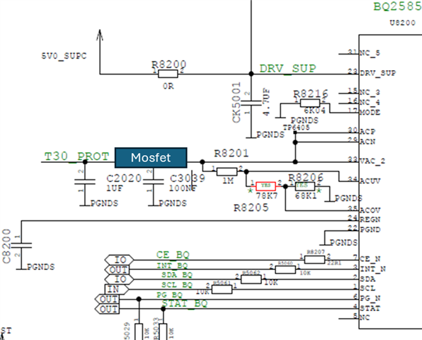
  1. 1.If input current detection is not implemented, do the ​​ACN and ACP pins​​ still need to be connected? Or can they be left floating?
  2. 2.Do the ​​ACN, ACP, and VAC​​ pins require ​​reverse polarity protection​​?
  3. 3.If only ​​buck-boost operation​​ is needed, but ​​bypass mode​​ is also required, can the ​​Q3 and Q4 switches​​ still be omitted?
  4. 4.In ​​Constant Current (CC) mode​​, are the ​​charging current value​​ and the ​​maximum charging voltage​​ set by hardware design, or are they both configured via the ​​I2C​​ interface?
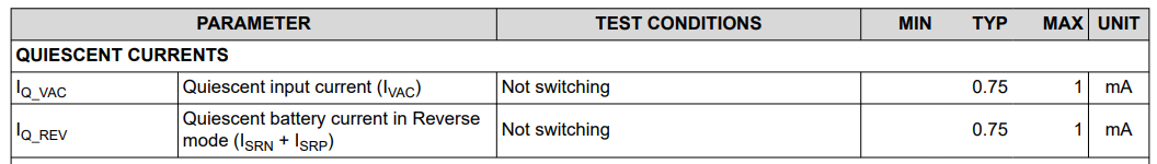
  5. 5.When the BQ25828 is not actively operating, does it have a ​​low-power mode​​ or ​​sleep mode​​? What is the ​​quiescent current​​ (in mA)? Which pin controls this mode?


  • Hi Frank,

    Thanks for working with this device.

    1. I would short these pins together and tie them to VAC.
    2. Yes, the BQ25858-Q1 does not have the ability to handle reverse polarity. The minimum voltage value is -0.3V.
    3. Q3 and Q4 are required for buck-boost. Did you mean buck only?
    4. The charging current and maximum charging voltage, or the CC and CV values of this device are configured via I2C. You can set a hardware limit of the input current and output current as a failsafe, however. The device will select the lower value of the two current settings.
    5. There is no sleep mode, but you can set EN_HIZ via I2C to turn off the REGN and stop switching. The datasheet lists the typical quiescent current as 0.75 mA and the maximum value as 1 mA.

    Let me know if there are any further questions.

    Best regards,
    Michael Bradbourne

  • schematic15b.pdf

    Hi thanks for information.could you please help check the SCH applicaiotion for 12V/20A, only bulk mode.

    another question is the DRV_sup can use internal Voltage, just link directly connect to REGN pin?

    thanks.

    best regards.

    frank 

  • Hi Frank,

    Thanks for working with this. I reviewed the schematic. Here are the notes:

    • The Coss of the MOSFET is too high. The BQ25856 datasheet has a section on power MOSFET selection that recommends the total switch node capacitance is less than 160/Vin (in nF). This is left out of the BQ25858 datasheet for some reason, but the information still applies. The MOSFET Coss here is 5.7 nF.
    • It would be helpful to place some ceramic (or other low ESR) capacitors close to the switching network on the T30 node
    another question is the DRV_sup can use internal Voltage, just link directly connect to REGN pin?

    This is correct. DRV_SUP can be from an external power supply. We also offer the REGN supply for DRV_SUP. When using REGN for the gate drive power, connect REGN directly to the DRV_SUP pin.

    Best regards,
    Michael

  • Hi, Michael

    thanks for feedback, for the typical quiescent current, if we add a mosfet on VAC pin to control VAC on/off,  could this reduce the quiescent current?
    when VAC off, how about the chip typical quiescent current?

    Best regards

    Frank zhang

  • Hi Frank,

    if we add a mosfet on VAC pin to control VAC on/off,  could this reduce the quiescent current?

    I think that the quiescent current would then depend on the MOSFET selection.

    when VAC off, how about the chip typical quiescent current?

    Do you mean that VOUT is still powered but VAC is not?

    Best regards,
    Michael Bradbourne

  • hi Michael 

    Do you mean that VOUT is still powered but VAC is not?

    yes,  Vout is still power,but VAC is not.

  • Hi Frank,

    The quiescent currents are the same:

    IQ_REV will the quiescent current when Vout is powered.

    Best regards,
    Michael