


Other Parts Discussed in Thread: TPS6287B25, TPS62870,
Tool/software:
dears,
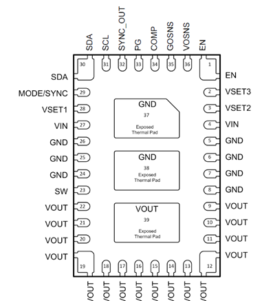
Our power modules, such as TPSM8287AXX, always have 3 thermal pads as below picture shows:
I checked the datasheet and EVM user guide, there is no detailed guidance on the PCB design and soldering skills for the PADs, just find a picture as below:
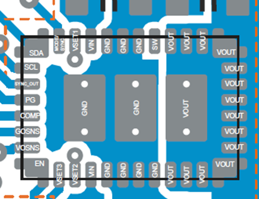
There are only 2 vias for each PAD-- but I find that the user guide of TPS6287B25 says to use 9 150um vias on the thermal pads, which is correct? I read some articles on the internet, they recommend multi vias to improve thermal dissipation capacity and <250um vias to limit the solder leakage, are they right? Should the customer use blind vias or put solder resist to the vias before soldering?
In addition, as the thermal pads are a bit big, it may cause the difficulty to mount the device on the PCB. How to secure the welding quality to avoid non-firm soldering? Should the 2 GND thermal pads on the PCB top layer need to be separated or prefer to combine them in a bigger plane?
Please help to share me the guidance on the PCB thermal pad & vias design and soldering process.
Thank you!

