TPS25751EVM: GPIO Events to control USB2.0 Mux for BC1.2 compatibility

Part Number: TPS25751EVM
Other Parts Discussed in Thread: TPS25751, TS3USB221A

Tool/software:

Hello,

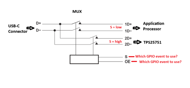
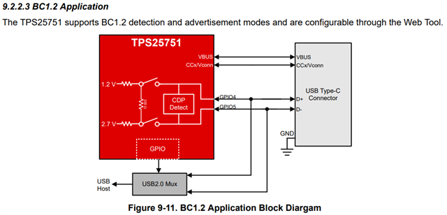
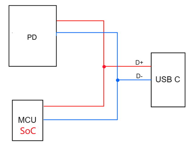
In our design we use TPS25751 (TPS PDC) for autonomous charger control. We need support of BC1.2 together with PD3.2. We use USB2.0 Mux to switch DN, DP between TPS PDC and our AP.

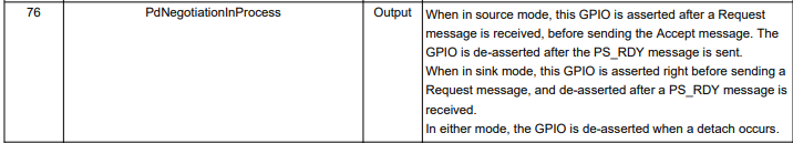
Which TPS PD GPIO Events to use to control S and OE inputs of MUX? Is it correct, to use PdNegotiationInProgress event for S input and Dp_Dm_Mux_Enable_Event for OE input? 

TS3USB221A Mux is used. Is it ok to use 100nF decoupling cap for MUX Vcc and power it from TPS PDC LDO_3V3? MUX Icc - max 30uA.

Thanks for the support!

  • Hello Vladislav,

    Thank you for reaching out.

    Is it correct, to use PdNegotiationInProgress event for S input and Dp_Dm_Mux_Enable_Event for OE input? 

    Dp_Dm_Mux_Enable Event is acceptable to use for enabling the mux. 

    From my understanding the GPIO is set high when the process for power negotiation is occurring. Then is set low once the negotiation is complete.

    For the MUX select pin behavior, will you want the MUX to change the D+/D- lines it's outputting to base on this behavior I have described above? See the datasheet description below for detailed description.

    Typically, the PlugEvent or the Cable_Orientation_Event is used for the select pin for the USB2.0 mux. 

    Thank you,

    Katilynn

  • Hello Katilynn, 

    Thank you for response.

    I want to use this scheme:


    I need D+ and D- USB 2.0 lines connected to our application processor AP but also want support of BC1.2 charging protocol. By the picture above MUX is connected to the  AP when S is low and to TPS when S is high. 

    The idea is that the MUX will switch to TPS for BC1.2 enumeration for a while after connecting the USB cable and then switch back to the application processor. And I need to know which GPIO event to use for that. So the event logic should be Low-High-Low.

    What GPIO events should I connect to the MUX control inputs so that DP and DN are switched to our application processor after the BC1.2 communication is completed, as described above?

    I can optionally leave the OE input permanently grounded so that the MUX outputs are always active.

    The manual also lists this connection:

    Here the USB data bus is split before the Mux and the Mux is not actually a Mux but just a switch to the USB host. I don't understand how the USB bus impedance of 90 Ohm is maintained when there is a Y-split to the TPS and a switch to the USB Host. Does this mean that after the BC1.2 communication is completed, the switch to the USB Host is switched on and at the same time the GPIO4 and GPIO5 inputs of the TPS are switched off to a high impedance state? What TPS GPIO event is used in this case to switch on the switch to the USB Host?

    Thanks for the support!

  • Hello Vladislav,

    Thank you for your response.

    Just to clarify, are you wanting to do USB data and BC1.2 at the same time? See the block diagram below for reference for routing. 

    Thank you,

    Katilynn

  • Hello Katilynn,

    Yes, I need USB data in the MCU and BC1.2 in the PD at the same time.
    The PD works in autonomous mode with a charger without communication with the MCU. The MCU will immediately perform Audio Accessory enumeration on the DN and DP pins after connecting the cable.

    Are you really sure that I can connect it like this?

    Won't there be a conflict between BC1.2 detection in PD and Audio Accessory enumeration in MCU at the same time on USB data lines?

    Thanks.

  • I will also add that the MCU does not know about the PD and they do not communicate with each other. So the MCU cannot have its pins in the HiZ state during BC1.2 detection in the PD.