Other Parts Discussed in Thread: TPS25980
Tool/software:
Hi TI team,
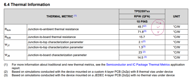
I’m using the TPS25974LRPWR on a 5 V rail at ~4–5 A max continuous. The RPW package has ~0.3 mm IN/OUT pads, and the datasheet examples appear to rely on via‑in‑pad and very small via diameters to move current and spread heat. My fab option doesn’t support via‑in‑pad or tiny vias at reasonable cost. I can get down to 0.15 mm drill and 0.3 mm OD with added cost but I’m hoping to avoid the cost overhead.
Can you provide any layout approaches to achieve ~4–5 A without via‑in‑pad or very small vias or via-in-pad on this package?
I’m especially interested in:
-
Preferred ways to share current top <-> bottom when vias must sit just outside the pads (e.g., short dog‑bone, via fences, copper “wings”).
-
Practical rules of thumb you use (e.g., short neck length targets, nearby via count/size/spacing, copper weight, and minimum pour area) for multi‑amp layouts on RPW.
-
Any reference layouts/app notes for this device/package that do not use via‑in‑pad or microvias.
-
If the above isn’t advisable, suggested alternatives with similar protection features but wider power pad geometry.
Board context (brief): 2-layer, 1 oz copper preferred; 2 oz possible; vias down to ~0.30 mm drill, pad ≥ ~0.45 mm (without added cost); finish ENIG. Fab is JLCPCB.
Application (brief): VIN/OUT 5 V, latch‑off circuit‑breaker variant, ILIM near roughly 4.5 A, inrush configured.
Thank you!
— Neil