Tool/software:
I'm working on a power supply design similar to to the evaluation board for this device. (HIgher switching frequency, wider input voltage range, therefore different magnetics; otherwise nearly identical.) My design is plagued by an overpowering additional signal riding on the primary-side current sense transformer. I thought this was caused by switching transients and coupled into the current sense signal due to poor PCB layout. I have since redone the PCB, and this signal has only become clearer. It increases with increasing input voltage. (This circuit needs to operate from 175 to 425VDC input at 468.75kHz SYNC frequency). And this unexpected current is typically several times the amplitude of the reflected secondary current signal, making it difficult to achieve stable current-mode regulation. I can improve this slightly by RC filtering of the current signal, but this is not a clean solution with this much "noise" to remove. See attached scope shot:

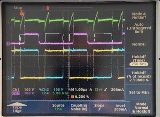
The upper (green) trace is the output of the primary-side current sense transformer. You can see the small reflected-secondary-current ramp overtaken by the much larger extraneous signal mentioned above. The second (magenta) trace is the center tap of the power transformer secondary (which is the input to the output LC filter). This shows that the offending current-sense signal ends at the rise of the secondary output voltage. The lower traces (yellow, cyan) are the left and right sides of the full bridge. You can see that the offending current signal begins at each transition of the left side (shim inductor side) of the bridge. In my hazy conception of the detailed sequence of magnetic activity, this would represent the energy transfer into and out of the magnetizing inductance of the transformer. And this might indicate that the transformer chosen has too little magnetizing inductance relative to the secondary-side low-pass filter inductance. But the transformer has a 6:1 ratio from primary to each side of the center-tapped secondary, has a primary-referred magnetizing inductance of 1.8mH, and the output filter inductance is 10uH. The primary-side-referred filter inductance would then be 36x10=360uH, which is five times smaller than the primary-referred magnetizing inductance. So the inductances would appear to be appropriately chosen.
What am I misinterpreting? Right now my intention is to move the current sense transformer from the primary side to the junction of the secondary filter inductor and capacitor (with appropriate rescaling), which I would think should entirely remove this overwhelming extraneous signal and permit proper current-mode regulation. (Do you agree that this should work?) But this leaves me with very large currents on the primary side which require larger bridge FETs, which means higher capacitance, which means more switching loss. I'd like to get rid of that unwanted current and slim down the primary FETs.