


Tool/software:
There are two major issues in the TPS92201A datasheet:
- Section 8.2.2.2 is copy-pasted from some other TI buck converter, and does not match anything else in the datasheet, and even specifies the feedback voltage as 0.6V (99mV is correct).
While TPS92201A could be used as a buck converter with PWM-scaled output, the description for this use case would need a reference schematic; the 8.2.2.2 as-is is just misleading.
- 8.4.2 Layout Example has mirrored layout for SOT563 (TPS92201ADRL). Unless you mount it upside down, or consider the layout as looking up from the bottom, it is impossible.
Both layouts ignore the fact that the LEDs are connected between FB and the other side of the inductor connected to SW (marked as VOUT in the Layout Example). This means the example layout is quite suboptimal.
I am not an EE or PCB design engineer at all, only do that as a hobbyist, but for a single-layer layout, I would consider for example
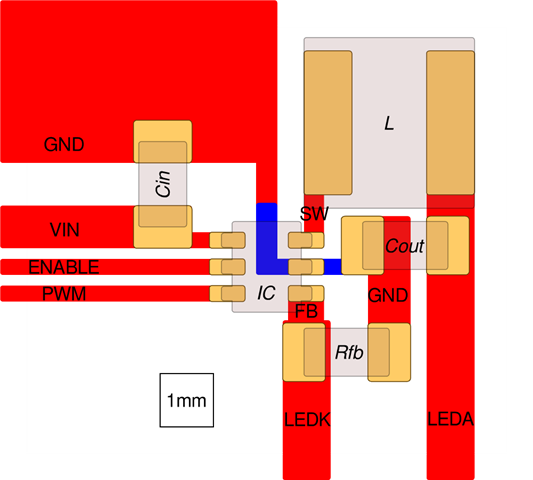 |
where the inductor is a 3mm×3mm package, and Cin, Cout, and Rfb are 0603 packages; the image is to scale, and you can download the original Inkscape SVG file from here (CC0-1.0/Public Domain). The blue region (partially underneath the SOT563 package) will carry full LED return current, so a proper multilayer design would use vias to the ground plane here; I consider it the weak point of this layout. As I do PCB design only as a hobby, I have not characterized this, I just wanted to post this so the comparison to the datasheet Layout Example makes the issues obvious. In fact, if there is a better layout example, I too would be interested in seeing that one.
