BQ76952:BQ7695202

Part Number: BQ76952

Tool/software:

I have been using the BQ76952 for half a year. During this period, I have also discovered some issues that cannot be completely resolved yet. Therefore, I am posting this to seek assistance from experts to solve them:
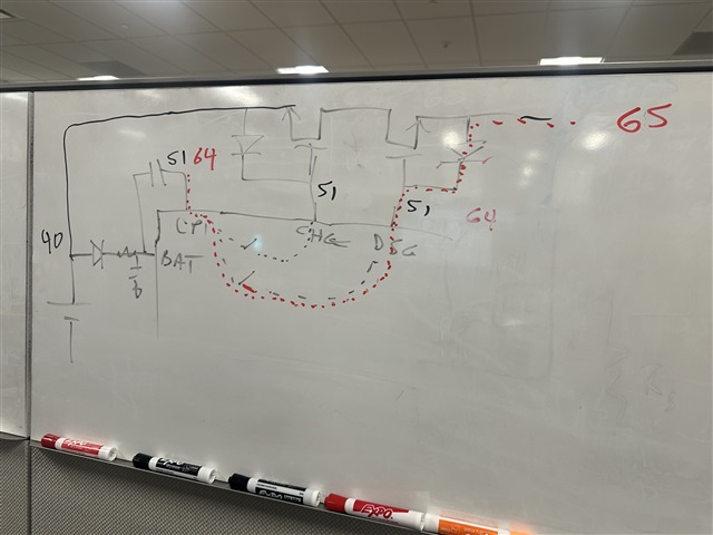
Architecture description: The MCU controls the working state of the BQ76952, and transmits data externally or updates the program for the MCU through RS485.

Question 1:
Problem Description: The program was burned into the MCU via RS485. During the initialization of the MCU, it was discovered that the equalization circuits of AFE were completely burned out.
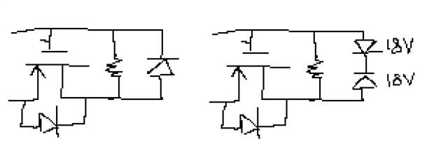
Preliminary Analysis: By measuring the burned PCB board, it was found that, for example, the voltage of VC1 was normally around 3.3V, but the actual voltage of VC1 was B+ voltage. Similarly, the voltages of VC2/VC3 were also like this. This led to a large power consumption of the filtering resistors in the equalization circuits, causing further burning.
Required Assistance: In principle, our burning-in of the MCU will not affect AFE. However, we have already damaged 3 boards, and currently we cannot determine the cause. We need experts to provide guidance and suggest possible reasons?

Question 2: Application scenarios of 16-cell battery packs,
Question description: When the battery cell voltage is 2V and the total voltage is approximately 32V, and a charging voltage of 60V is applied to P+ and P-, artificially creating a voltage difference of more than 20V between the charging voltage and the total cell voltage, it is found that the charging MOS transistor has burned out;
Preliminary analysis: After multiple re-tests, the reason for the damage of the MOS transistor is that when the voltage difference is greater than 20V, the charging MOS will have a driving voltage of about 4V, causing the MOS transistor to be in a slightly conducting state. As a result, the loss of the MOS transistor will be very large, and the MOS transistor will be damaged;
Things needing assistance: May I ask, when the charging voltage is more than 20V above the total voltage of the battery cell, why does the charging MOS transistor have a driving voltage? What is the cause of this and how should we solve it?

These two issues have been bothering us for two months now. We really need expert explanations and solutions.

Thanks Very much.

  • I am very much looking forward to the support from experts and also to their prompt response.

    thanks.

  • Hello,

    Question 1:

    Is there a schematic you can share?

    Question 2:

    Are you using the integrated high-side N-channel MOSFET drivers? Or the digital outputs DDSG and DCHG for low-side? What is Settings:FET:CHG Pump Control [LVEN] configured to?

    Regards,

    Rohin Nair

  • AFE_Protect.pdf

    1、For details, please refer to the attached drawings.

    2、The CHG Pump Control is activated immediately after power-on. This feature has been verified through hardware testing.

  • Hello Gaojie,

    Question 1:

    Please give me some time to go through schematic.

    Question 2:

    I have just updated Jiaqi regarding this question. I believe what may be occurring is that your CHG FET is off when your charging is occurring. Currently, you have the diode protection for your CHG FET as shown on the left. Try adding another diode and let me know if this fixes your issue when charging with 60V. This is shown on the right.

    Regards,

    Rohin Nair

  • Question 1:If you need a complete circuit diagram, Manager Wang has it.  it is not convenient to upload it here.

    Question 2: I think you misunderstood my meaning.

    The test procedure is as follows: 1. The BMS enters a sleep state, and the total voltage of the cells is 40V. The external charger sets the voltage at 65V, resulting in the voltage at the Pack end being 25V higher than the total voltage of the cells.

    2. We have added a logic for not charging when the pressure difference is too large. When the pressure difference exceeds 25V, the charging mosfet of the BMS board will not be opened, but the voltage of the charge pump will rise from 11V to around 20V. The discharge MOS gate will gradually generate a driving voltage of about 3V. A driving voltage of 3V will cause the MOS transistor to be in an incompletely conducting state. A pressure difference of 20V will result in a transient current of 600A. Under the condition that the MOS transistor is incompletely conducting, the MOS transistor will be damaged.

    The issue that needs to be addressed now is: why does the charge pump voltage rise when there is a 20V pressure difference between the pack  and the Bat ? Why does the charging MOS have a gradually increasing voltage of Vgs?

    As shown in the above figure, it should be to clamp the driving voltage with positive or negative voltages. However, this cannot solve the problem we are currently facing.

    Looking forward to your reply. thanks.

  • Hello,

    I understand now. Please give me some time to go through this again.

    Regards,

    Rohin Nair

  • Thank you for your reply. We still hope to receive some guidance as soon as possible.

  • Hello,

    I apologize for the delay. I am still discussing with the team on what could be occurring here, and we will get back to you on this.

    Regards,

    Rohin Nair

  • May I ask if there are any results yet?

  • Hello,

    I am still discussing with the team. I will get back to you as soon as I can.

    Regards,

    Rohin Nair

  • Hello,

    Several days have passed, and we still hope to provide possible outcomes and improvement measures. We are very much looking forward to your reply.

    Thanks.

  • Hello,

    I think the following image might better explain what is occurring:

    Does this make sense?

    Regards,

    Rohin Nair

  • I think I can understand why the damage occurred, but I still don't have a strategy on what to do. How can we prevent the voltage of CP1 from rising now? When the CP1 voltage rises, why does it cause the charging MOSFET to have a Vgs voltage? Could you please clarify exactly what we need to do? We can take the time to verify it.

    Thanks Very much.

  • Hello Gaojie,

    Adding another diode in reverse as shown above should prevent the CP1 from rising. Can you try adding this and see if this issue still occurs?

    Regards,

    Rohin Nair