TPS63802: Part fails after few months of normal operation

Part Number: TPS63802

Tool/software:

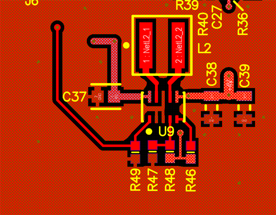
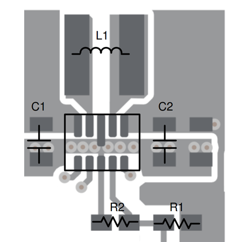
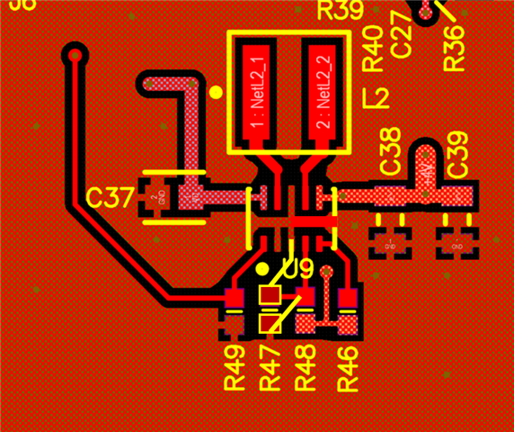
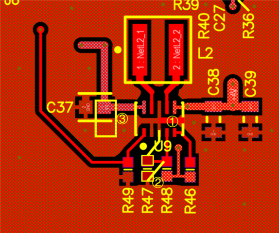
A regulator is built using TPS63802DLAR. It takes the power (VD on schematic) from a single Li-Ion cell and converts it to 4V. A typical load current is 300-500mA with very short bursts up to 1A. The enable signal is 0V/2.5V. About 1000 boards were built, and so far two parts failed after several months. Once failed, they take sink about 100mA from the power source even with the enable pin at 0V. The enable function still works, i.e. there is 4V on the output with enable pin high and 0V with enable low. I am attaching the schematic and the layout. The PCB has four layers with a massive ground pour on the top and bottom plus the ground plane with frequent vias, so the part doesn't get hot.

What can go wrong?

  • Hi Vladimir,

    The two failed parts has normal function to regulate the Vout, but they will additionally sink 100mA, right?

    Please check the following items:

    1. Is there a AB swap experiment performed? I'd like to check does the sink current follow the chip or the board?
    2. For the failed units, please measure the resistance between the VIN/VOUT/L1/L2 pin and GND pin.
    3. If available, please check the voltage at the L1 and L2 with enough bandwidth. 

    Regarding the schematic and layout.

    • No concern on the schematic. But for the layout, the major one that should to be improved is that connect the GND pin and the Cout GND at the same layer. And also, the input cap and output cap can be adjusted to put more close to the chip.
    • You may refer to the following layout example.

    Regards 

    Lei

  • The failed unit has an idle current of 101mA at 4V. The good unit current is 107uA, and that includes the standby current from multiple parts, not just the regulator in question.
    Here are the resistance values measured on both units.
    1. Vin to GND - both high, over 3 MOhm
    2. Vout to GND - good board 70 kOhm, failed board 21 Ohm
    3. L1/L2 to GND - good board 2 MOhm, failed board 1.8 MOhm
    I was unable to capture the L1/L2 voltage  because after 10 - 15 minutes it took me to do the above measurements, the IC failed entirely, the supply current went to 0.5A, and the IC started smoking. It appears that when the device was running from the battery that was limiting supply current, the IC was falling slowly, but once I connected it to the benchtop supply with low output impedance, it failed entirely quickly.
    I removed the IC from the failed board and Vout to GND resistance went to 75 kOhm, which I think proves that this is the issue with the IC, and not with control or the downstream parts.
    Please let me know if I can do anything else to expedite solving this issue.
  • Hi Vladimir,

    I'll check and reply to you tomorrow.

    Regards

    Lei

  • Hi Vladimir,

    Thanks for your information. It seems that there is a resistive path formed between the VOUT and the GND pin in the chip, so on the failed units the 4V Vout can still be regulated but with an abnormal big idle current.

    With a bad GND trance, the main power path from VOUT pin --> Cout --> Cout GND --> GND pin is long. So the spike at the SW and the Vout may be big to damage the device.

    To verify this, could you run an good unit with the same work conditions and measure the voltage at the L1, L2 and VOUT with enough bandwidth quickly (within 10 minutes)?

    Regards

    Lei


  • Hi Lei,

    The Vin is a DC level between 3.7 and 4.2V depending on the battery capacity. It can get to 5V exactly when the battery is charging, but the regulator is disabled in that state.

    The Vout is close to 4V, almost perfect DC.

    The waveforms for L1/L2 are below. They were taken at Vin = 4V, full load, vertical scale 2V/div, two horizontal scales. The yellow trace is L1, and the red trace is L2.

    Thanks,

    Vladimir

  • Hi Vladimir,

    I'll check and reply to you by tomorrow.

    Regards

    Lei

  • Hi Vladimir,

    Please zoom in one or two L1/L2 switching cycles, with so the overshoot/undershoot ring can be more clear.

    And also, do you know what's the bandwidth of the oscilloscope probe? Usually it's 20MHz. While, to measure the spike accurately, it's better to have the bandwidth >= 250MHz, or the measured spike will be smaller than the actual value.

    Go back to the waveforms you measured, the max spike seems no problem, but the min (negative) spike looks close to -3V already. That can be explained because of the GND trace in the output path is not good.

    Except the GND trace, I also noticed that the feedback GND (R47) is not good. In current version it's simply connected to the GND plane, so the feedback GND may be noisy. If there is a chance to optimize the layout, please don't forget here. Following is an example: rotate the R47, connect the R47 GND to the GND pin with a separate GND trace.

    Regards

    Lei

  • Hi Lei,

    I use 100MHz probes with 100MHz scope.

    Here is a zoomed-in waveform:

    Unfortunately the waveform varies significantly from cycle to cycle, so I went back capturing multiple waveforms with Vmin and Vmax measurements enabled:

    As can be seen Vmin = -2.835V and Vmax = 6.537V with 100MHz bandwidth. I am sure if I would use a 250MHz bandwidth, the voltages would be higher. Can such short pulses actually damage the IC? Does that confirm your hypothesis?

    Thanks,

    Vladimir

  • Hi Vladimir,

    If the -2.835V is less then 10ns, then should be no problem.

    And the Vmax 6.537V with short duration is also ok.

    Will it be possible to have a new optimized layout version and keep on monitoring first?

    Except the 2 failures, are there any new failure encountered?

    Regards

    Lei

  • Hi Lei,

    Yes, we will be changing the PCB to your recommendations, but this is a complex product currently in production, so before we make any changes, we need to determine the root cause of failure.

    Looking at my data and your responses I realized that there is an alternative way of measuring the voltage over L1/L2. I was trying to capture a single period or a few periods, but the voltage changes randomly, and the chance of capturing the worst period is pretty low. So instead of doing that I set my oscilloscope to 1sec/div, 500ks/sec to acquire as many periods as I can and measure minimum and maximum. The waveform is attached. It appears that the minimum is -3.188V and the maximum is 6.62V. Unfortunately this method doesn't allow determining how wide are the minimum and maximum. Would this data be useful for you to tell me how we are damaging the regulator?

    Thank you,

    Vladimir

  • Hi Vladimir,

    From the measured data, the concern is in the low spike of -3.188V. I think it can also be reduced by the layout optimization.

    Regarding the layout optimization, there are three items total, shown below:

    1. GND trace
    2. FB GND
    3. Cin position

    The most critical item is the first one: GND trace.

    Before the formal layout update, you may have a quick check first: scrape out the solder mask layer and connect the GND (shown in ①) by solder, and then check whether the low spike is reduced.

    Regards

    Lei