Tool/software:
Hello TI Team,
I am facing multiple issues with my UCC28711DR-based flyback design(50W) and would appreciate your guidance.
Schematic:
Layout:
Background
Design Specs: Input is 40V-800V DC, 50W Power.
-
Initially, I tested the circuit using a controlled DC source at the DC bus.
-
The IC started switching at around 55 VDC (possibly due to peaks).
-
However, it kept restarting repeatedly, so I increased the DC bus to 100 VDC.
-
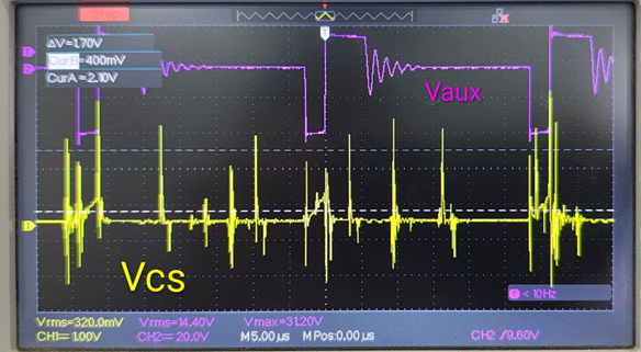
Waveforms for this condition are attached (Fig1, Fig2, Fig3).
-
-
My auxiliary and secondary windings are designed for the same output voltage (15 V).

Fig1
Fig2
Fig3
Problems Observed
Problem 1:
-
The output is regulating at 23 VDC instead of 15 VDC, even though the number of turns for both the auxiliary and secondary windings (Naux and Nsec_15V) are identical.
Problem 2:
-
The VS pin seems very sensitive.
-
When I touch the divider node (between RS1 and RS2) — not directly the pin — the output voltage sometimes increases, and then the IC turns off and restarts.
-
Even when not touching, bringing a metal tweezer close to this point causes disturbances.
-
I am unsure whether this sensitivity is expected behavior of the VS pin, or if it is due to my PCB layout.
Problem 3:
-
After modifying the CS pin divider, the IC kept restarting, so I checked the CS waveform (attached).
-
To rule out the DC source, I switched to an AC variac connected to a diode bridge:
-
Applied single-phase AC at 60 VAC (DC bus ~80 V).
-
The IC continued to restart.
-
Changed the VS divider (RS1 = 51 kΩ, RS2 = 22 kΩ) to increase current at the VS pin.
-
-
Divider values were calculated as per the datasheet table.

Fig4
Fig5
Fig6
Table calculation was followed as per pdf: /cfs-file/__key/communityserver-discussions-components-files/196/slua783.pdf
| VAUX_RMS_measured | 12.8 | V |
| RS2 | 22 | k |
| RS1 | 51 | k |
| DIVIDER RATIO_calculated | 0.301369863 | |
| VS PIN_calculated | 3.857534247 | V |
| VDC_OUT_measured | 20.89 | V |
| VAUX_PEAK_measured | 30 | V |
| VS PIN PEAK_calculated | 9.04109589 | V |
| VS line-sense run current (IVSL_RUN_NEEDED) | 225 | uA |
| VS line-sense stop current IVSL(stop) | 80 | uA |
| Absolute Maximum Peak current, VS (I_VS) | -1200 | uA |
| IVSL_RUN_CAL | 250.9803922 | uA |
| IVSL_RUN_CAL(from peak) | 588.2352941 | uA |
| Maximum switching frequency fSW(max) | 100 | kHz |
| desired time for tON fault is 1 / FSW(max) | 10 | us |
| LPRI_designed | 70 | uH |
| IPRI_measured | 0.1 | A |
| VBLK_measured | 40 | V |
| for the first cycle, tON_calculated = (LPRI × IPRI ) / VBLK | 0.07 | us |
| Minimum CS threshold voltage VCST(min) | 195 | mV |
| Maximum CS threshold voltage VCST(max) | 780 | mV |
| RCS | 235 | mohm |
| Min peak primary current IPP(min)_calculated | 0.829787234 | A |
| Max peak primary current IPP(max)_calculated | 3.319148936 | A |
Current Status
-
Unfortunately, one IC was damaged while I was measuring voltage at the VS pin.
-
Although I did not short it, the multimeter probe introduced noise which caused the IC to fail.
-
So far, I have lost five ICs this way. I am waiting for replacement ICs to continue testing.
Request
Please advise on:
-
Why the output voltage is regulating much higher (23 V) than the expected 15 V.
-
Why the VS pin is so sensitive to nearby objects/noise, and whether this is normal or a layout-related issue.
-
How to stabilize operation and avoid continuous restarts.
Any recommendations to help me operate the UCC28711DR in a normal and stable manner would be greatly appreciated.
Thank you.
Best regards,
VIKAS