TPS25730: Is TPS25730D connected DRAIN PAD to GND problem?

Part Number: TPS25730

Tool/software:

Hello TI -Team,

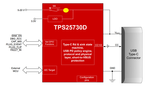
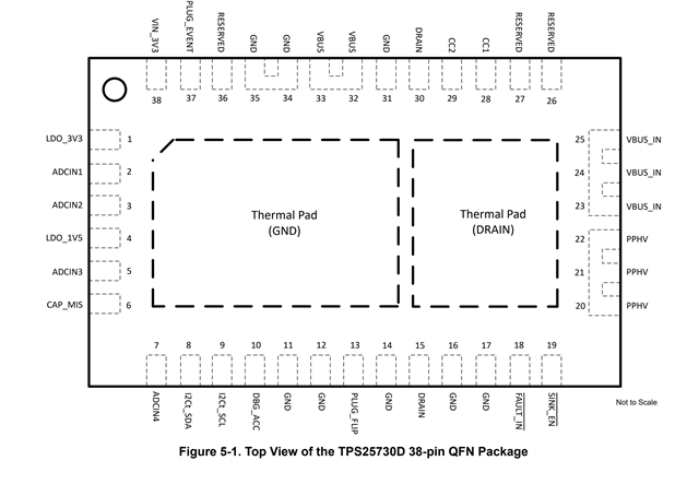
i crated schematic with TPS25730D and i have problem with the initial test. The device is not working. I take a look in the layout from the supplier and noticed that the DRAIN PAD is connected on the Footprint with ground. The Drain Pin is not explicitly connected in the schematic. Can be that the Problem?

  • Georgi,

    Yes, not connecting the Drain/Drain_Pad pins (or rather connecting them to ground) would be a problem. The D package of this device has the FET for the PPHV (power path high voltage) integrated. The way you have described the schematic, you essentially have the yellow dot from the picture below:

    ... Connected to ground. This means your VBUS line is shorted to ground. A way to confirm this would be to take a handheld multimeter and see if your ground pin and your VBUS line are connected.

    The drain pad is used primarily for thermal considerations. As the FET is internal, the heat generated from the RON on the internal FET needs to be dissipated somewhere- and it is done so via the thermal pad of both GND and DRAIN. You have the right idea for the layout with the copper pours, but it needs to be separated into two pours to match the footprint of the device:

    Best Regards,
    Tim

  • Hello Timothy, thanks for the answer. Problem is resolved.