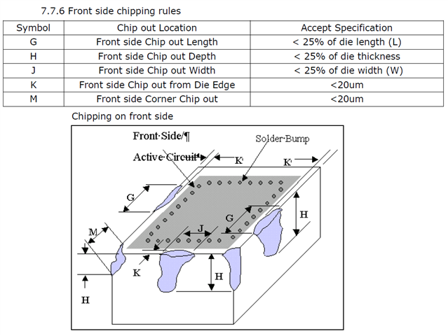
Tool/software:
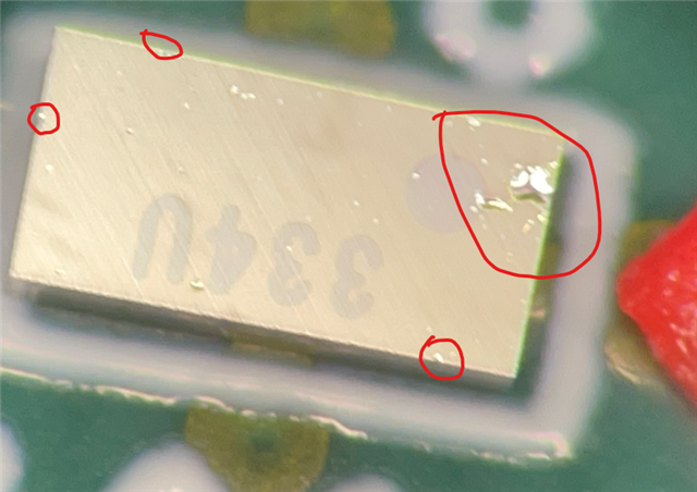
We are seeing a wide range of chip outs on the component body (post SMT processing) and we would like to under if there is an acceptability requirement.
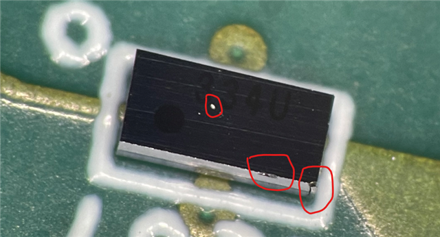
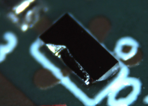
Tool/software:
We are seeing a wide range of chip outs on the component body (post SMT processing) and we would like to under if there is an acceptability requirement.