Tool/software:
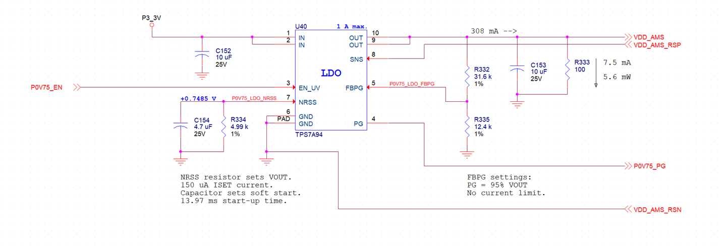
Please review this schematic for the TPS7A94. It is one of six implementations of the LDO that I have in my design, with VOUTs of +0.75 V, +0.8 V, +0.9 V, +1.5 V (two instances) and +1.8 V.
For this schematic:
- VOUT = +0.75 V @ 308 mA max.
- NRSS resistor = 4.99 k, 1%
- The 100 ohm resistor from VOUT to GND is a bleed resistor.
- EN is controlled by a power sequencer IC and is a +3.3 V signal.
- Despite the low output current, the IC being powered by the LDO actually has differential voltage sense outputs, and these are implemented in the schematic.
- The + sense line goes to the SNS pin.
- The - sense line goes to the TPS7A94 GND pin. I need to know if this is correct.
- 10 uF, 25 V ceramic input and output capacitors.
- SS and FBPG values calculated from data sheet.
- Thank you!