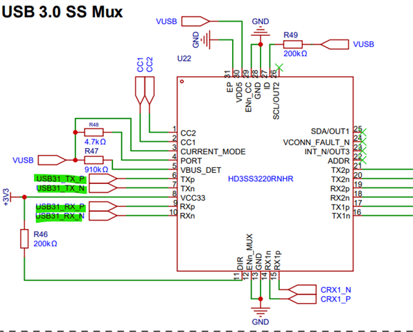
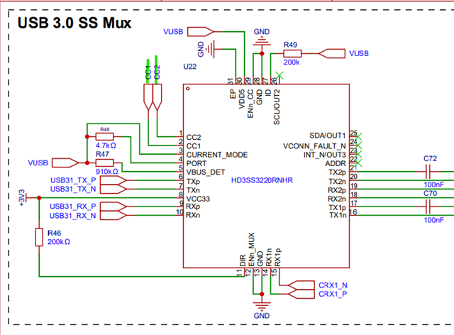
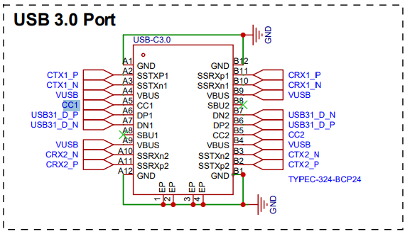
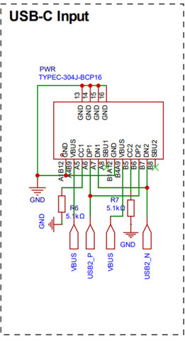
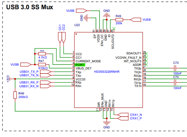
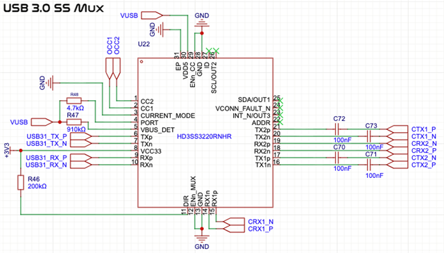
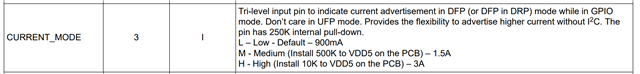
Part Number: HD3SS3220
Tool/software:
Hi!
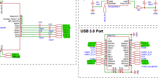
In response to the previous thread I have updated in lieu of the changes suggested and just wanted a review of my schematic and layout before fabrication.
Schematic:

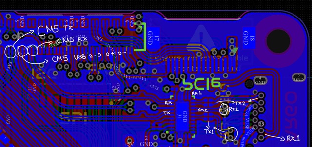
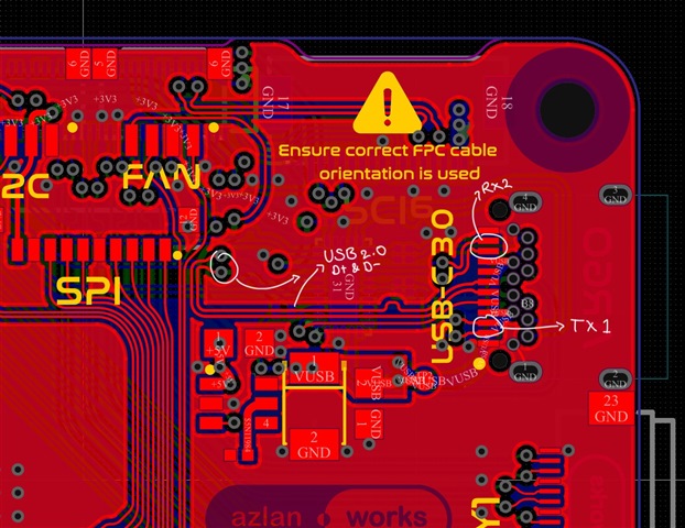
Layout:
Layer 1:

Inner Layer:

Bottom layer

The PCB is 6 layers:
SIG/GND : GND : SIG/PWR : PWR : GND :SIG/GND
All signal layers have a ground power but I have removed them from view for easier readability. Would really appreciate feedback on the schematic and layout as well as power to the USB-C port!
Thanks