UCC20225: Anomalies at Gate Driver High Side Pulses

Part Number: UCC20225

Tool/software:

Hi TI Elites,

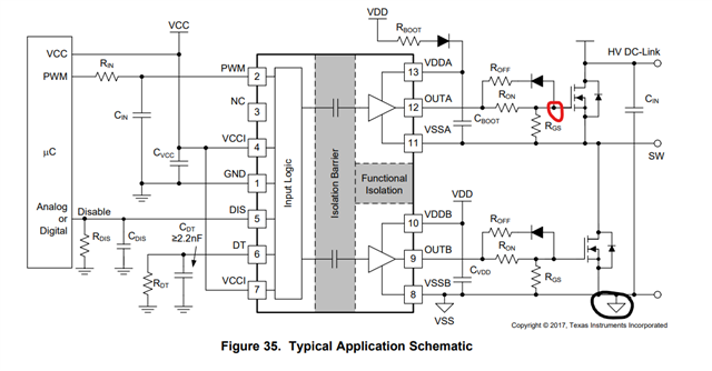
I'm using UCC20225 to drive my two-phase stepper motor. As my understanding gate driver HS and LS are inverting with each other which mean

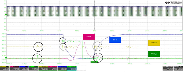
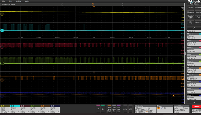
I expect to see signal on the HS when the LS is being turned on too. But I found out there is extra pulses at the low side when I zoomed in my waveform as shown below.

How does this happen? Could you please provide some advices?


Legends:

Yellow: Motor Output Current 
Cyan: Gate Driver HS 
Red: Gate Driver LS 
Green: Input PWM 
Orange: The other Gate Driver LS 
Blue: Current sense amplifier output (Configured as in-line setup)
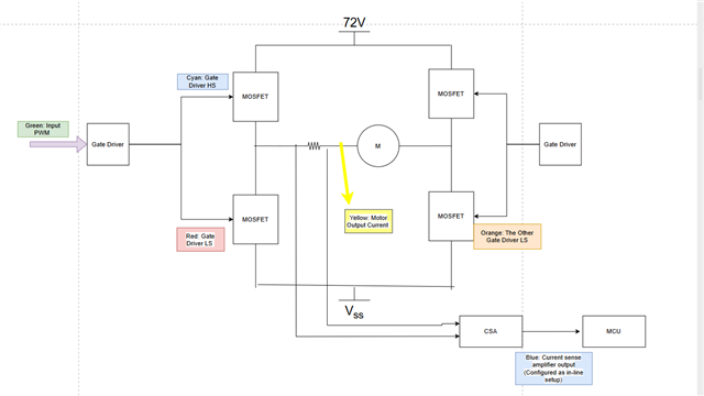


Driving Settings:
Motor Supply Voltage: 72V 
Driving Frequency: 100kHz 
Driving Ipeak: 4A

  • Hi Jun,

    The LS channel (red) appears to be following the correct output structure, but the HS channel (cyan) looks quite different. I noticed that the orange channel (other gate driver LS) appears to be mostly following the expected behavior of what the cyan channel should be outputting.

    The cyan channel also appears to be really high in voltage with peaks of 80V. This is out of datasheet absolute maximum ratings, and could possibly result in gate driver damage. Can you confirm the supply voltage for VDDA (assuming A channel connected to HS), and ensure it is within spec? If it is, I would also recommend to check the HS MOSFET to ensure it is not accidentally supplying voltage to the gate driver HS output channel.

    Best regards,

    Will

  • Hi Will,

    Q: Can you confirm the supply voltage for VDDA (assuming A channel connected to HS), and ensure it is within spec?
    A: Yes, I'm supplying 12V for the secondary supply, and the probing is as the figure show below.


    I couldn't understand very well for your second statement: 
    " If it is, I would also recommend to check the HS MOSFET to ensure it is not accidentally supplying voltage to the gate driver HS output channel."

    Can you provide some illustration for better understanding?

  • Hi Jun,

    What I meant is that if the MOSFET is broken, it could be possibly shorted from G-D or G-S. If the MOSFET is not broken, then we need to analyze the gate driver behavior a bit closer. Would you be able to provide a waveform of OUTA with reference to VSSA? In order to verify the behavior of OUTA, the waveform of OUTA needs to be referenced to VSSA. If possible, try to probe as close as possible to the gate driver output pins. This applies to both OUTA and OUTB.

    Best regards,

    Will

  • Hi Will,

    Q:What I meant is that if the MOSFET is broken, it could be possibly shorted from G-D or G-S. If the MOSFET is not broken, then we need to analyze the gate driver behavior a bit closer.
    A: How should I inspect to know that my MOSFET possibly shorted from G-D or G-S? As what I know, I know it's short and beeping when I am probing continuity mode on Drain & Source at the same time by using multimeter.

    Q: Would you be able to provide a waveform of OUTA with reference to VSSA? In order to verify the behavior of OUTA, the waveform of OUTA needs to be referenced to VSSA. If possible, try to probe as close as possible to the gate driver output pins. This applies to both OUTA and OUTB.

    A: The OUT A (Cyan) and OUT B (Red) already presented at the very first image posted. Both references are with VSS

  • Hi Jun,

    It seems like your MOSFET may be damaged. If possible, I would try to substitute it out for a new one and see if the issue persists.

    In the question above, I am asking for a waveform of OUTA with reference to VSSA (SW node), not VSSB. Is this how you are probing when measuring for OUTA? Since you mentioned both references are with VSS, and in the image above VSS is tied to VSSB, so I wanted to clarify that OUTA is being probed with reference to VSSA and not VSSB.

    Best regards,

    Will

  • Hi Will, 

    Thanks for waiting.

    I have changed to differential probe to measure OUT A with reference to VSSA and OUT B with reference to VSSB. 

    I have been probing wrongly all the time that's why it show more than 80V as my reference is OUT A to VSSB. 

    So the MOSFET still working fine. as the photo attached below. The circled part is showing there is ringing on the CSA output and PWM at the same time domain. 


  • Hi Jun,

    I'm glad to hear you were able to determine the MOSFET is working properly. If there are any other questions about using UCC20225 your system, please let me know and I would be happy to help.

    Best regards,

    Will

  • Hi will, do you have any ideas how to solve the ringing stated from the above?

  • Hi Jun,

    If your probing is as close to the gate driver pins as possible and the above waveform is what it looks like, then I would suggest to try to filter out the noise ringing as best as possible. It is difficult to tell where the source of the noise is, but I would start by looking into all affected pins as a start. I recommend taking a look at VCCI and PWM pins first, since the noise appears to be on the primary side.

    Best regards,

    Will