UCC28180: Power derating for line votlage below 100VAC

Part Number: UCC28180
Other Parts Discussed in Thread: TL431

Tool/software:

Hi TI team,

I have a question about analog boost PFC controller IC "UCC28180". I want to implement a power derating for the line voltage values below 100VAC (rms). In case of Vin < 100VAC_rms, i want to limit the average current (and hence the input power of PFC). If it is possible I want to force the current loop to limit the average current through the inductor to a fixed value. if the load tries to draw more current, then the output voltage drops under its set value.  

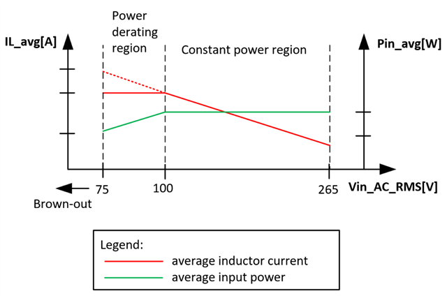
Figure 1: aimed power derating behaviour

As you can see in figure 1, in normal case the current will looks like the dotted line (between input voltage range 75-100VAC). But I want to limit it to a fixed value, which will cause input power derating. To achieve such behavior, one need to saturate the current loop. I think if I can limit the pin 5 "VCOMP" by clamping it to a fixed voltage when line voltage falls below a certain value, the current loop cannot command more than a given value. And if load increases beyond that current value, the output voltage will drop. 

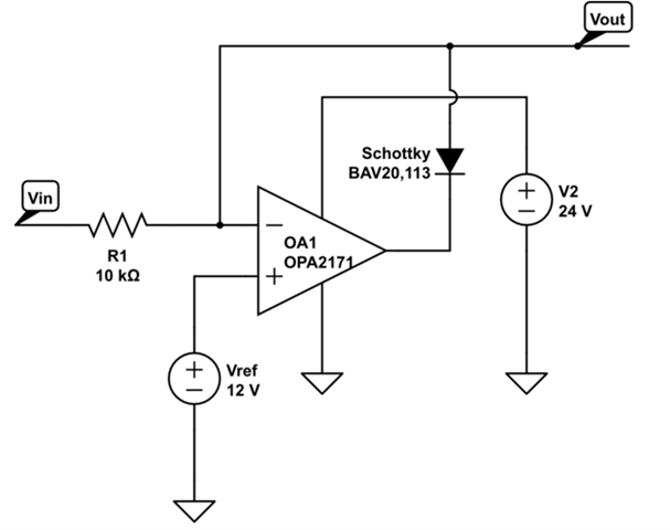
Figure 2: Hardware implementation

Can I implement such circuit to clamp voltage across VCOMP pin? Will it work? Can IC provide enough current for the zener diode? May EDR (enhanced dynamic response) function cause problem? Do you have a solution for such implementation?

best wishes 

Süleyman

  • Hello Suleyman, 

    I think that in principle, your idea can work.  In practice, it may be a little difficult to reproduce the same power limit over thousands of units due to tolerance variations.

    The Zener-diode clamp is the simplest implementation, but Vz variations or VCOMP variations may result in some "soft" power limit, not exactly the same from one unit to another. It might also change over temperature within one unit. 

    An op-amp-based clamp with TL431 regulator for a reference can be a more accurate and repeatable clamp, but is a little more complicated, similar to this: 

    (Diagram borrowed from: https://electronics.stackexchange.com/questions/248308/op-amp-diode-clamping-circuit )

    Here, Vref would be the TL431 clamping voltage (< 5V), Vout goes to the VCOMP pin.  Vin and R1 are open circuit.  The diode does not have to be Schottky; can be p-n. 
    The form of the circuit is important.  The actual specific components used are not so much important, as long as they can handle the stresses involved.

    EDR current will have to be accommodated, but its maximum current is -275uA (out of the pin) so it shouldn't be too difficult to clamp. 

    Regards,

    Ulrich

  • Hello Ulrich,

    Thank you for your reply. I have another question for your suggested circuit. Do I need to put a resistor between resistor and diode to limit the current? VCOMP pin connected to output of the internal transconductance amplifier (votlage amplifier). Should the current flow limited? If yes, on which current value should I limit?

    Best regards 

    Süleyman

  • Hello Süleyman,

    A resistor in series with the diode is NOT necessary because the UCC28180 transconductance amplifier output current is self-limiting. 
    As I mentioned, the maximum current out of the VCOMP pin can only be 275uA or less. 

    Regards,
    Ulrich

  • Hello Ulrich,

    Thank you very much.

    Best regards

    Süleyman