UCC21750-Q1: nFLT pin fault conditions

Part Number: UCC21750-Q1
Other Parts Discussed in Thread: UCC21750

Tool/software:

I'm troubleshooting a half bridge module that uses two UCC21750s. After a few minutes under load, the low side IC will assert the fault pin, stopping operation. On the control side, the fault and reset pins from both ICs are tied together, and this net is pulled up to 3.3v with a 1kOhm resistor. As part of troubleshooting, I've lifted the desat pin off the board and bridged it to the adjacent com pin, to disable the desat circuitry on the low side.

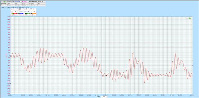
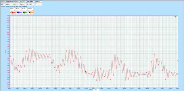
In spite of disabling the desat circuit, the fault pin still goes low after a few minutes. If I lift the low side IC's fault pin off the board, the circuit will operate under load indefinitely. In the scope image below, the green trace is the fault line (250mV/div), red is current through the device that's faulting (50A/div), yellow is the current out the midpoint of the bridge (25A/div), and blue is an unused probe. The timescale is 50us/div. The green probe was a standard 10x probe with a clip lead on it, in a fairly noisy environment. The packaging of the system means I can't use a spring clip or hold a probe in place, sadly.

The only schematic different between the LS and HS is that AIN/APWM are used on the HS to sense module temperature. On the LS, AIN is tied to COM and APWM is floating. The fault consistently occurs on the LS IC.

I've reached the limit of what I can learn from the datasheet, so I'm hoping y'all have some suggestions or insight into what else could be causing the fault pin to go low.

  • Hi Michael,

    Thanks for the detailed message on the system observation and highlighting that the FLT low observed when DESAT is tied to COM.

    Can you please confirm whether the FLT behavior is device dependent or does it happen on multiple devices/boards?

    Also please share if the FLT observed only during certain load current or always?

    By looking into the noise profile of the FLT signal, looks like the system is very noisy. In case of noisy system, it is recommended to follow the best schematic and layout practices.

    Can you please check the  recommended schematics and check if the application schematics and layout has any major differences from the recommended.

    Looking forward for your inputs to understand the scenario and improve the system behavior.

    Thanks

    Sasi

  • Thanks for the response!

    It happens on a few boards, but not the majority of them.

    The FLT has only occurs under load, as you might expect, higher loads appear to fault quicker. 

    The schematics are quite similar. I've soldered a few additional low value capacitors to the circuit so we match all of the required components, the circuit already included most of the recommended parts and some optional ones as well. The additional capacitors didn't appear to change anything.

    Our component sizes don't match the ones in the layout example, so there are differences, but I have read through the recommendations and optimized the layout to minimize the size of the critical loops, place critical components close together, and the design includes the recommended primary and secondary ground planes.

  • Hi Michael,

    So based on your inputs, the failure is observed on specific devices/boards only. To understand if the issue follows the device, have you tried replacing the device which shows FLT to a good board and a good device to the failing board.

    This will help to eliminate any board level variations.

    Also i want to understand whether the high current path DC+ to DC- is separated from the gate driver. Especially we recommend DC- to be maintained as separate plane and COM to be separate plane and it needs to be connected through Star connection - not as a single plane.

    If the failure follows the device, i would request to plan a small 10pF (HV cap) across GND and COM of the failing device to understand if the issue goes away for debugging purpose.

    Looking forward for your inputs.

    thanks

    Sasi

  • Sorry for the delay, I've been repeating the various test conditions to make sure the results are consistent. Sometime it can take 3 hours to fail so repeat tests take a long time. In repeating the tests, I've noticed that the fault only occurs when the system is under load, but the specific half bridge module is approaching a zero crossing (this is an AC application).

    Since the application is a half bridge module, and the fault only occurs on the low side, I swapped the HS and LS UCC21750's and neither faulted. I believe this means there is some minor variation in the UCC21750 that the design is making act out.

    The connections to the devices are all kelvin connections and the high current path is separated from the gate drive circuitry. 

    I haven't added the additional capacitor since the failure didn't follow the device. Capacitance across the isolation barrier is typically a thing to be minimized in this application, but I will see if I have a small capacitor to try this with the failing configuration.

  • Hi Michael,

    Thanks a lot for the detailed update on different approaches you tried. Yes there can be some minor variation between part to part. Based on your explanation, low side device was more vulnerable and when switched to high side, fault didn't occur.

    Yes, it will be very helpful if you can confirm if adding cap across the low side gate driver when it is in low side position. 

    Thanks a lot for working with us on understanding the failure reason. Really appreciate it.

  • Again I'm sorry for the delay, we ordered some capacitors to use for testing and yes, adding the capacitor across the low side IC does consistently stop the fault from occurring. 

    I'll try to measure the common mode slew across the gate drive, though I won't be able to probe it at the instant of the fault.

  • Hi Michael,

    Thanks for confirming that the 10pF cap across the GND and COM on the low side driver helps to stop the FLT from occurring. It will be good to capture the voltage across the gnd without cap to understand the noise profile when the FLT is occurring. This will help to understand the frequency component which causes this behavior. Pls use 1Ghz probe (at minimum 500Mhz BW) with smaller ground loop to reduce measurement noise.

    Also signal capture of the waveform with the CAP (10pF), to confirm if the noise profile is different without cap.

    Thanks again for your continuous effort to narrow down the system behavior. Looking forward to hear from you and we would love to work with you to understand the root cause of this behavior and help enable the system robust.

    Thanks

    Sasi

  • Sadly I'm a bit limited on the measurement equipment I have. The best measurement I can make at the moment is using a 200MHz isolated scope and a passive probe with a typical ground lead. With that, the peak slew rate I've measured is 357V/us with or without the 10pF capacitor (the probe itself has a 5.5pF input capacitance). The pk-pk voltage of the measurement is 1552v and the location is obviously in the vicinity of several high power connections, so it's a bit challenging to find a high speed probe that can be attached close to the board (i.e. no hand-holding) and supports the voltage necessary.

    The fast ringing appears to be in the range of 150kHz, which I don't have an explanation for yet. There's a slower speed square wave near 10kHz due to switching, and at the midpoint there's a single large transition again due to switching.

  • I was able to solder a BNC connector across the IC to reduce the noise picked up by the probe. The result was very similar, with a significant peak at 135kHz but not much beyond that.

  • Thanks Michael for the measurement and sharing it with us. Is it possible to share the waveform version of this file for both with 10pF cap and without 10pF cap.

    It will help us to analyze the waveform better.

    Thanks again for your support. In terms of your system solution. As the observation is only applicable for a specific unit only and you could position it in highside instead of low side. Is that right?

    Thanks

    Sasi