


Tool/software:
Hello,
We are using TPS2066D to control VCC supply to USB 2.0 connector which connects to bus-powered or self-powered USB devices. The intention is to supply 5v on USB VCC (VCC_USB0_C) when a bus-powered USB device is connected (such as thumb drive) through OUT1 pin and disable OUT1 output when a self-powered device (such as a laptop) is connected on the same connector. The OUT1 pin is enabled/disabled by switching the USB0_OTG_ID signal as shown in the snippet of the schematic below.
By default the circuit is in "device mode", where USB0_OTG_ID is pulled to 3v3, disabling the 5v output on OUT1 pin.
When a self-powered device is connected the circuit is in "device mode", USB0_OTG_ID stays at 3v3, OUT1 output voltage stays low and 5v is supplied on VCC_USB0_C from the external device.
When a bus-powered device is connected the circuit switches to "host mode", USB0_OTG_ID is grounded, pulling EN1 to 3.3v and enabling 5v across IN pin to OUT1 pin to supply the external USB device on the same VCC_USB0_C line .
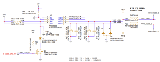
We have found 2 TPS2066D that have been damaged and we suspect this may be due to the fact that when we switch from "host mode" to "device mode" there may be a brief moment when 5v still supplied from OUT1 pin and 5v coming from an external device momentarily which may be the cause this fault due to a reverse current across OUT1->IN pins. As I understand it there is no internal reverse current protection for TPS2066D.
Can you see any issues with driving the circuit in this way? Perhaps there is a way to estimate the maximum reverse current that TPS2066D can handle before failure?
Best regards,
Arturas Kazenas
