


Tool/software:
As I continue working on this challenge (thankfully my client has been patient), and following the recommendations shared here, I have adjusted the values, used a resistive load, and modified the Excel data to accomodate the control loops requirements, but I’m still not getting the required results.
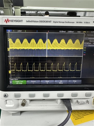
After sharing the schematic here and confirming that it looked fine, the test for an input of 300VAC (intended 220VAC~480VAC) and a constant output of 705Vdc with a resisitve load of 653Ohm (no e-load available and no use of regenerative poewer source to test; at light load on current test for this ocassion, it is intened for 6.6kW tho~), the waveform on the gate for the SiC transistors (4-pin) is as below:
I initially assumed the issue was related to the PWM Ramp and Offset network, but that seems unrelated to the driving stage.
I understand that the UCC28070 gate driver is clamped at 13.5Vdc. I also added a ZXGD3002E6TA 5 A peak driver in a BJT totem-pole configuration for faster switching.
Shouldn’t the Vgs waveforms be square, and the gate driving voltage level reflect the supply (I am using 14 V DC to feed all analog circuits)?
My second question is more related to testing. Should this PFC be tested only at no-load or full-load conditions? What I mean is that I’m trying to observe its behavior at light load, where I would expect around 705 V DC output, but it is not reaching that value.
Thank you in advance for your support.