LM5122: SW Input pin margin seems too tight if boosting to 100V

Part Number: LM5122

Tool/software:

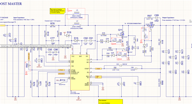
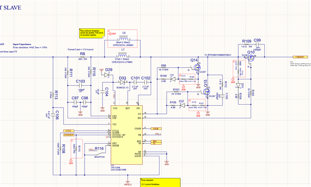
I currently have a 1500W boost design using a pair of LM5122. I'm boosting from a nominal input of 48V to 100V out. 

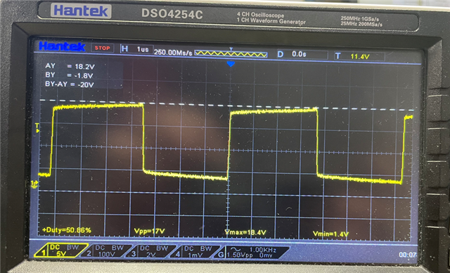
Generally, I have things working pretty well, however occasionally I'm seeing a failure that so far has been hard to narrow down. When the failure occurs, I generally lose all my FETs (high and low side) as well as the LM5122 ICs. I'm not sure which fails first but I'm starting to question if the issue is with the SW pin. I see there is an absolute max of 105V on that pin, referenced to AGND. The datasheet says the part is designed to boost up to 100V but I that margin seems very close for comfort. 

I get a very stable 99-100V output after the high side FETs (at my bulk capacitance) but I see above 100V at the SW pin. 

Do you have any recommendations for ensuring the SW pin doesn't see more than 105V when boosting to 100V? Or should this part actually be avoided when needed 100V out?

  • Hello Brian,

    thank you for using E2E.

    Can you share your schematics, please?

    Did you use our recommended Quickstart calculator for your design? LM5122-BOOST-CALC Calculation tool | TI.com

    best Regards,

    Johannes

  • Here are snippets from my schematic, master and slave configuration. I'm using a 30uH inductor currently with a large saturation current rating.

    Yes, we did use the design tool initially. This design is based on those calculations. 

    We're running at a pretty low frequency (140Khz) in order to reduce heading in low side FETs but the ripple current shouldn't be out of hand. 

    I appreciate your thoughts! 

  • Hi Brian,

    Thanks for the explanation and the schematics.
    I did not see any problems within the schematic structure.
    The main issue is like you already pointed out: The abs max rating of SW is 105V, while your typical SW rises to 100V.
    Meaning any overshoots of more than 5% will come with a risk of damaging the device.

    Unfortunately, we do not have any other synchronous boost controllers in our product line portfolio that can support higher switch node voltages. The next best option would then be to switch the whole topology to a system more suited for 1.5kW power ratings.

    For now, would it be possible to you to take a waveform measurement of the SW voltage?
    If the overshoots are still very small or can be further reduced through snubbers or higher gate resistors, the application might still work out, but in general there is still a high risk for device damage as the margin to the abs max limit is simply too small.

    Best regards,
    Niklas

  • Here is a scope capture after bumping the voltage down to 93V for continued testing. This is captured with a differential probe across AGND and the SW net plane (I can't easily get right at the pin so it might see something slightly different). 

    The scope probe is x50 so you need to multiple the values by 5x to get the true voltages. I don't notice any/much overshoot @ this voltage. I do see a shift on the GND side which I'm not positive if it's real or not but based on the amplitude (18.4V x 5 = 92V) it does look like it is real. Otherwise, I would be seeing slightly less voltage at the output (Meaning if 17Vpp was the total swing I would only be seeing ~85V at the output).

    Is there any protection that could be put right on the SW pin in order to help? Ex. Small series resistance, etc?

  • Hi Brian,

    Thanks for the waveform.
    I agree with you that there seems to be no overshoot at in this measurement.
    The GND shift is rather confusing. I would consider a GND shift of ~10V rather abnormal, so I would expect this to be a measurement artifact and not the actual pin voltage.

    Regarding the protection circuit, a series resistance is not recommended.
    It would require a clamping circuit to prevent any voltages above 105V.

    The best solution would be to use external drivers that are rated for 120V or higher. These external drivers take the LO and HO signal from the LM5122 devices and there is no longer the problem with the device abs max rating, as the SW voltage is fed to the external drivers directly.
    This will increase component count and needs a layout change, but high efficiency can be maintained this way.

    Best regards,
    Niklas

  • Thanks, Niklas, 

    Do you have any example schematic or example part number to look at for the external driver you mention? That might be a good path forward if we decide we HAVE to have 100V boost. At the moment, I'm testing with a slightly boost voltage of 93V to see if the issues go away (to try and confirm the failure is related to the SW pin). 

    Do you just mean an external gate driver IC?

    Thanks again!

    -Brian 

  • Hi Brian,

    I checked for reference design internally but did not find suitable matches for this case.
    The problem is that I am not a full expert for external drivers.
    We have several of these within the TI portfolio. For example, this one could be a good fit:
    https://www.ti.com/product/UCC27282

    For implementation, the SW pin of the LM5122 controller is shorted to GND. The supply of the UCC driver can be taken either from an external voltage or directly from the LM5122 VCC.

    I can offer to review the design once the first revision of the schematic is available.
    For questions on the best suitable UCC device, you can open a new e2e thread in parallel to get feedback for an expert on this field.

    Best regards,
    Niklas