LMG1210: LMG1210 'grounding' in Class-D amp design

Part Number: LMG1210

Tool/software:

I'm trying to design a single-supply Class-D BTL audio amplifier using two LMG1210 to drive four GaN HEMPTs.  In such designs, it is usual to have separate ground planes for the 'analogue input' sections (which include the PWM generator circuits) and the (more noisy) 'power' output section (the HEMPTs).  The LMG1210 interfaces between those sections, and the two ground planes need to be connected, preferably at a single point.

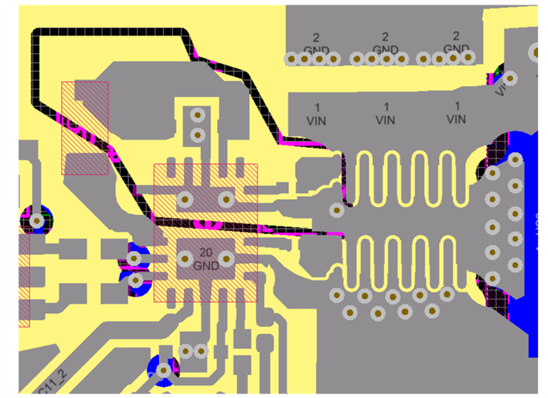
The LMG1210 has two Vss pins (plus a Vss thermal pad).  Is it OK to rely on the internal connection between these pins to link the two ground planes (e.g. connect analogue ground plane to pin 3 and power ground plane to pin 7)?

Related to this, the LMG1210's Vss pad is used to help dissipate heat from the chip.  Given that the 'power' ground plane will serve a similar purpose for the (much hotter) HEMPTs, would it be OK to connect the LMG1210 Vss pad to the 'analogue' ground, to provide better overall cooling?

Thanks, Daniel

  • Hi Daniel,

    The LMG1210 is a single ground driver. For the LMG1210EVM layout (shown below), both VSS pins are tied to the VSS thermal pad (in grey), and then both planes are tied to the common ground plane (in yellow) below. We do recommend to tie both VSS pins to the thermal pad in the layout.

    Thanks,

    Annabelle

  • Annabelle, Thanks for this, but it does not answer my question of whether I can use the LMG1210 to provide a single link between the 'quiet' (input) ground plane and the physically separate 'noisy' (output) ground plane, the LMG1210 being the interface between these two amplifier sections.

    Or are you suggesting that the LMG1210 has its own little ground plane, which then connects either side by single track links (or vias, or ferrite beads) to the other two ground planes?  Or are you saying there's no point having physically separate (but electrically linked) ground planes for the 'quiet' and 'noisy' sections, and I should just have one big ground plane used by low- and high-power components?

  • Hi Daniel,

    From the driver perspective the most important care-about is to have the gate drive loop (high-current carrying path) as short and close to the driver as possible to minimize trace inductance. This can be achieved using a ground plane and having the FET as close as possible to the driver to have a solid and short connection between the FET and VSS pin/VSS power pad through the ground plane. If this is taken care of, then from the driver's perspective, connecting the other VSS pin to the controller side GND or connecting both VSS pins to the same ground plane shouldn't make a significant difference.

    Thanks,

    Annabelle