


Other Parts Discussed in Thread: BQ25505, TPS22919, , TPS22992
Tool/software:
Hello,
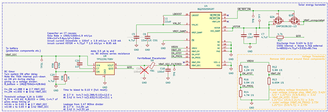
I am trying to find a solution to discharge a capacitor node of a battery boost charger IC prior to startup of my system and thought about utilizing a load switch with external QOD option.There is bi-directional energy transfer between a battery, the boost charger and the system load which would need to go through the load switch.
Specifically I am using the TI BQ25505 energy harvester which has an output node called VSTOR that needs to be at <100 mV prior to hot plugging a battery or the chip will not power the system. Unfortunately, it is quite hard to connect the battery without having a short disconnect (bounce) when inserting the battery mechanically or connecting a power jumper. Hence, the output node gets charged on the first connection and causes the chip to prevent power to the system after the bounce event. Only a full discharge and replugging the battery will eventually power the system up.
I asked a previous question on the BQ25505 forum which led me here.
Specifically I identified TPS22992, TPS22917, TPS22919 to be suitable for this application (maybe there are other options as well). Combined with a simple delay RC circuit it could first discharge the VSTOR node through QOD and then close the load switch and power up the system.
Please find a sketch of the application below. In a battery discharge scenario the energy goes from left to right.
I have a few questions about this application:
- TPS22917 has a reverse current protection which triggers at 500 mA. The charger will not supply more than 500 mA peak to the battery. Nevertheless, it sounds like a bad idea to use the chip in reverse current mode.
- TPS22919 and TPS22992 don't have the reverse current protection but draw more Iq (8 uA and 10 uA respectively) than TPS22917 (0.5 uA). I am trying to keep the Iq of the whole system <100 uA leaving these options as viable but not ideal.
- TPS22917 datasheet does not specify leakage on QOD during normal operation (ON). I assume it is sufficiently high but I also don't want leakage during normal operation and discharge duration can be quite long. Hence an additional resistor to the internal 150 Ohm of 4.7kOhm was added.
- TPS22917 datasheet states that the recommended min turn on voltage for ON pin is V_IH = 1V. However, Figure 7-5. ON Pin Threshold gives me 0.65V. I will use that.
- There is no internal connection between Vout and QOD pins as shown in 9.2 Functional Block Diagram right? I am asking because this would bypass the boost charger in my case.
- Is there anything I am overlooking in "abusing" QOD for this type of discharge application?
- Is there a more suitable load switch or startup sequencer with integrated delay functionality instead of RC delay circuit by TI? I don't like that the RC circuit itself does not discharge itself automatically within reasonable time and a bleed resistor causes leakage.
Thank you for looking into this
Best regards
Tom