


Tool/software:
Hello Texas Instruments,
Just as in the title: Does BQ7791504 have cell balancing?
I am asking the question because I made a PCB for the BQ77915 series and tested (and deployed it) successfully using BQ7791500 and BQ7791501. I wanted to use the same board with BQ7791504 for a power demanding project because it does not have over-current protection, but had a surprise when I tested the balancing using a severely un-balanced pack. I got no activity on the balancing leds during charging. Balancing occurred only in an over-voltage condition. So here goes...
The schematic is designed for a 5 cell pack, with variants for 3 and 4 cell packs (0R resistors in specific locations).
Balancing uses external transistors and resistors, + leds for activity indication. The first observation of the balancing behavior (or lack of it) was made using a 3s pack with one cell way higher than the others (cell 2 had 4.1V, cells 1 and 3 had 3.6V). I removed the cells and switched to power supplies.
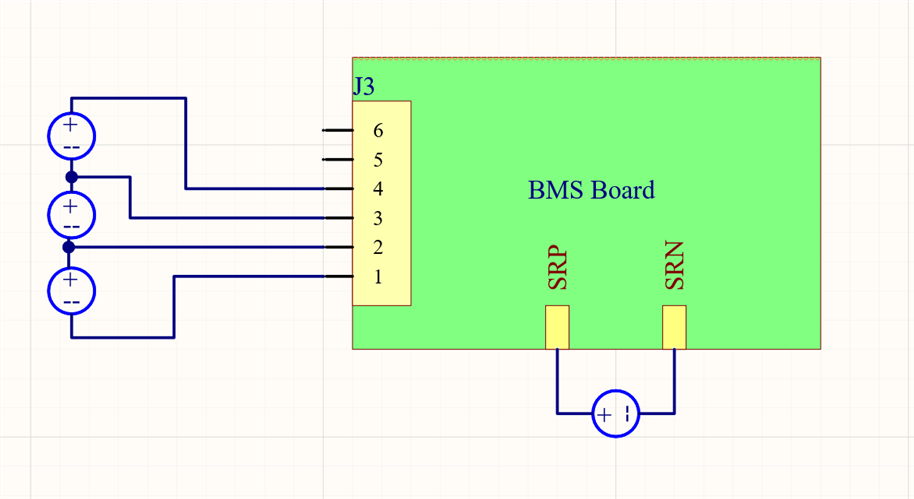
The test uses 4 isolated lab power supplies: 3 of them are connected in series to simulate the cells and the fourth passes a current through the sense resistor to simulate charging or discharging.
The test setup is depicted below.
The balancing test procedure starts with a discharged battery. The 3 power supplies will be set at 3.3V and the fourth will push current through the sense resistor in the charging direction. The cell voltages will be increased above the minimum balancing threshold, and after that one "cell" will be set higher, to create a delta above Vstep (50mV in the case of BQ..04). Balancing should occur, assuming there are no other errors and the voltage across the sense resistor is above the charge qualification threshold 1 (1.875mV).
Now the data...
Start the power supplies that simulate the cells, at 3.3V, starting with cell 1 and ending with cell 3.
Measure the voltage at P+ and P-: there are 9.9V at the output.
Measure the CHG and DSG pins, referenced to VSS pin: there are ~9V. Power mosfets are conducting.
Start the charging simulation power supply. The sense resistor is 2mOhms. The leads are connected to create a voltage from SRP to SRN (positive lead to R15, negative lead to R16). The voltage is set to 0.5V, the current limit is set to 2A. This will create a voltage of 4mV, higher than the charge qualification threshold 1 value.
The pack is now charging. The fact that CHG and DSG pins are both high indicates that there are no errors.
Next: increase the voltage of each cell above the balancing threshold. Starting from the bottom, each "cell" is brought up to 3.6V.
Next: simulate cell imbalance:cell 2 is increased in 10mV steps, until balancing occurs. Expected result: above 3.65V, the LED should illuminate. Actual result: no activity.
I continued to increase the voltage. Only at 4.277V, balancing occurs. The BQ is now in over-voltage mode: CHG pin is now low (0v), showing that charging is blocked. Maintaining 4.28V at cell 2, after disabling the 4th supply (injecting current across the sense resistor) the LED still blinks, so the cell is still balancing. This is another indication of over-voltage.
Next: reduce the cell voltage, 10mV at a time. At 4.167V (my supply has 7mV offset) the LED stops blinking. Over-voltage is finished, we are now in normal mode.
I tested this behaviour with all three cells, with the same result.
Here is what I checked:
- cell configuration: CCFG pin is set LOW, 0R resistor to VSS.
- TS pin: used a 10K resistor instead of a thermistor, for test purpose. DSG and CHG pins would not be both HI if there would have been an over/under-temperature condition.
- cell voltage measurement: checked that each VCx pin had the correct voltage, directly at the BQ pin. No problems here. Also, VC3=VC4=VC5=VDD.
- CBI pin: is set LOW, connected straight to VSS. Also checked the solder joint under microscope and re-soldered it, just to make sure. The behaviour was the same after re-testing. Also, according to pg 19 of the datasheet, the balancing fet of a cell in OV is turned on if CBI is LOW, so cell balancing is not inhibited.
- AVDD pin: ~3V.
- V(SRP-SRN): ~4mV. Charging qualification is met.
- PRES pin: pulled up to VDD with a 10K resistor.
So, what am I doing wrong?
I also attach below the schematic in PDF format. I can also provide the design files or the PCB if necessary.