LMR43610: LMR43610-External Component Placement Issue

Part Number: LMR43610


Tool/software:


Hi,

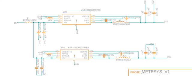
We're experiencing issues with our LMR43610MB3RPER integrated circuit in the power layer of our project. We've used the same schematic in different locations within the same project without any problems. The problem is located on the C9 top and R6 bot, which are connected to the integrated circuit. The integrated circuit is powered by 15V, and upon startup, Vout=1.5V quickly overheats and burns out. Despite replacing the integrated circuit twice on two different PCBs, the results are always the same.

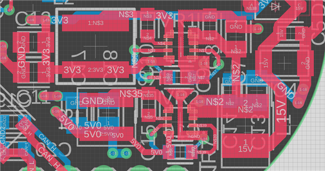
In our other circuits, the C9 top and R6 bot are present, and there are no problems. We're wondering if the issue is solely due to the placement of these two components on the PCB layers, or if there's a different issue.

The LMR43610MSC5RPER integrated circuit, shown in the PCB image, located in the same area, has no problems and operates without issue.

I await your feedbacks.

Best regards.

Halid.

  • Hello Halid, 

    I will discuss this query with our team, but i do have couple of questions. Is it only VR1 that is having issues and VR2 is showing no issues? When you say you have used the same schematic on different project with no issues, was the PCB lay out also the same on the different projects? Specifically were vias also used to route the VCC capacitor? Have i identified the C9 capacitor correctly in the bottom image? 

    Regards, 

    Oscar Ambriz 

  • Hi Oscar,

    Thank you for replyand support.

    Yes that' right. Only VR1 has issue, VR2 works perfect. 

    I have used same schematic on diffrent projects with no issues, was the PCB lay out has diffrences.

    I added the highlighted routes of C9 and R6 visually.

    Best Regards.

    Halid.


  • Hello Halid, 

    Looking at the differences between the two converters I see VR1 appears to have a larger VCC capacitor trace loop. Typically we recommend VCC be as close as possible to the converter but the primary reason is to minimize the parasitic inductance. Is it possible to measure the voltage at the VCC capacitor on both converters, it would be good to compare both waveform to verify no short is occuring at the VCC pin. In your initial request you stated that the problem was located at C9 and R6, how were you able to pinpoint that the failure was occuring at this location? 

    I also a larger inductance was used on VR1, is this because the output load is less than VR2? could a test be ran using the same inductance on both converters. 

    Regards, 

    Oscar Ambriz 

  • Hi Oscar,

    The reason I think there's a problem with the placement of components C9 and R6 is that there's only a difference in layout between them and the circuit in VR2, and the VR2 circuit operates without any problems.

    When I measure the VCC pin voltages of VR1 and VR2, both voltages around 3.3 volts. VR1-VCC=3.21V, VR2-VCC=3.27V.

    By the way, the difference in inductances is due to the load differences, but I haven't connected any loads to either circuit yet.

    Best Regards.

    Halid.

  • Hello Halid, 

    Both voltages are similar which is good. Are you able to measure the current through the inductor? I see you say that no load has been applied but it would good to verify that the inductor shows no signs of current pull. 

    Additionally, could you probe the switch node of the converter prior to the failure. I see you are operating the converter in auto mode, the switch node should show signs that we are in this mode of operation when no load is applied. 

    Is there a dedicated ground layer on your board, or are there only two layers? I see both converters don't have much of a ground trace to dissipate heat, but it does appears that the failing unit has more ground which is good. 

    Regards, 

    Oscar Ambriz 

  • Hi Oscar,

    Our PCB has a ground layer, and the images are attached so you can select the components.

    A photo of our board is attached. I'll remove the 8.2uh L2 inductor and measure the current. I'll share the information with you as soon as possible. Are there any other measurements you'd like?

    Regards.

    Halid

    .   

  • Hello Halid, 

    Current through the inductor and a capture of the switch node should be fine. 

    Regards, 

    Oscar Ambriz