LM5122: The LM5122 is not operating as expected.

Part Number: LM5122


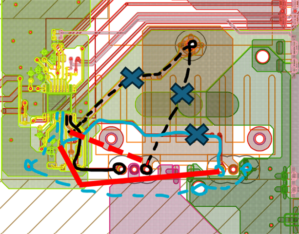
Hello. I am currently designing a circuit using the LM5122. I have built a prototype based on the attached schematic and am in the process of verifying its operation.

The input voltage is set to 24 V, and the target output is 53 V / 15.1 A. The circuit operates normally up to 10 A output, but when the output current reaches around 11 A, abnormal switching behavior occurs.

Could you please review the design and let me know if there are any issues or improvements I should consider?

I have attached the waveforms of Q600 (CH2) and Q601 (CH1) at 10 A and 11 A output conditions. 
circuit.pdf 

10A Load.png11A Load.png

Thank you for your support.

Best regards,
Nomura 

  • Hello Nomura,

    Thanks for using the e2e forum.
    Based on the schematic, current sense resistance and slope compensation look okay, so it should not be related to overcurrent protection.
    Output capacitance and compensation should be okay as well, so it should not be loop instability either.

    As this is a two phase design, do you see this behavior on both phases, or only on the primary phase as per waveforms?

    Would you also be willing to share the layout of the application?
    If this is a noise related issue, we might find further clues by reviewing the layout.

    Thanks and best regards,
    Niklas

  • Hello Niklas

    Sorry for the delayed response.
    This phenomenon occurs only on the master side (Q600/Q601).
    In the attached waveform, CH1 corresponds to Q601, CH2 to Q603, and CH3 to Q602.
    When the gate resistors of Q601/Q603 are changed to 15Ω and those of Q600/Q602 to 10Ω, the abnormal oscillation disappears.
    Could this be due to noise from the oscillation?
    I will send the layout data separately, but based on the above, do you see any possible causes?


    Best regards,
    Nomura 

  • Hi Nomura,

    Thanks for the update.
    Seeing the two switch nodes side by side, it should not be a problem of the oscillator or the switching frequency.
    I you just look at the falling flanks of the primary side HO signal (yellow), they match with the rising flanks of the secondary side HO signal (green). There are minimal delays, but these are not abnormal. The switching frequency is correct.
    The problem is that the primary side duty cycle shows two very long on-times, followed by a very short minimum on-time cycle. The PWM duty cycle is the problem.

    Higher gate resistances with slow down the slopes and reduce noise on the switch node.
    For example, if we assume the root cause is noise within the system that triggers unintended overcurrent protection, it will lead to minimum on-time cycles, which are then followed by very long cycles for compensation.
    This would explain why higher resistances or smaller switch node noise can improve the behavior.

    I am looking forward to the layout files to confirm this.

    Thanks and best regards,
    Niklas

  • Hello Niklas

    I've attached the layout data. Please check it and make any suggestions for improvement.

    B面シルク.pdfB面.pdfA面シルク.pdfA面.pdf

    Best regards,
    Nomura 

  • Hi Nomura,

    Thanks for the attachments.
    The power stage placement looks okay to me. The IC is placed away from the noisy power stage, so there should be no interference here.
    The traces of the current sense lines for CSP and CSN are also okay.

    The traces of the gate driver lines show some weaknesses.
    - We recommend to place the driver signals not directly below the switch node polygon.
    - We recommend to place the gate driver path and its according return path very close to each other. This means LO and PGND close together, as well as HO and SW.
    I marked the gate driver paths in the schematic and added their return paths with a dotted line:

    On the secondary side, the driver traces also also directly below the switch node, however, here the driver path and the return path are closer to each other, which is slightly better.

    Non-ideal driver path can lead to noise within the system, so it is possible that this leads to the unsteady duty cycle behavior.

    Best regards,
    Niklas

  • Hello Niklas

    Would it be better to take the high-side SW terminal from the source of Q601? (red dashed line)
    Is it preferable for the low-side gate line to be closer to the blue dashed line? (red solid line)


    Best regards,
    Nomura 

  • Hi Nomura,

    You are correct. The red dashed line for the return path of the HO signal would be a large improvement.
    Same for the LO gate signal. The blue dashed line shows the return path from the source of the MOSFET to the PGND pin of the IC.
    Not all GND polygons are shown in the schematic, so I just assumed there is a complete GND plane on another layer and I drew a straight line from GND via to GND via. Hence, the red solid line would be an improvement as well.

    Best regards,
    Niklas

  • Hello Niklas

    I am currently evaluating the existing PCB for the upcoming new model.
    The current model operates with a 24V input and 53V/12A output.
    The new model will also use a 24V input, but the output will increase to 53V/15A, resulting in higher power.

    In the current model, both low-side and high-side gate resistors are set to 22Ω, which causes significant MOSFET temperature rise.
    To improve thermal performance, I tried reducing the gate resistance, but this led to abnormal oscillation.

    I would like to lower the gate resistance as much as possible to reduce temperature rise, and I’m seeking advice on this matter.
    I have received pattern layout suggestions, which I will take into account during PCB design.
    The PCB design for the new model is scheduled to begin in about two months, and I would like to request a pattern check at that time.

    Regarding the power increase, the only planned change in the circuit is a slight increase in the capacitance of the input/output electrolytic capacitors.
    Other parts of the circuit will remain unchanged.

    Best regards,
    Nomura 

  • Hi Nomura,

    Thanks for the update.
    I can understand that high gate resistance will strongly increase losses and is not desired.
    If the oscillation can be avoided by improved layout and the gate resistance can be lowered, it would be a good solution.

    Feel free to send me the new layout once available and we will do a review from our side.

    Thanks and best regards,
    Niklas